Common Mistakes in PCB Design Work and How to Avoid Them
Printed Circuit Board (PCB) design is a complex process that requires careful attention to detail and adherence to best practices. Even experienced designers can make mistakes that lead to costly rework, manufacturing delays, or even complete board failures. This article explores the most common errors in PCB design work, categorized by design phase, and provides practical advice on how to avoid them.
1. Schematic Design Errors
1.1 Incorrect Component Footprints
One of the most frequent and costly mistakes is using wrong component footprints in the schematic. This occurs when the symbol in the schematic doesn’t match the physical dimensions of the actual component. The result is a PCB where components either don’t fit or have incorrect pin spacing.
How to avoid: Always double-check datasheets for mechanical dimensions before assigning footprints. Maintain a verified component library and implement a review process for new footprints.
1.2 Power and Ground Connection Errors
Designers often forget to properly connect power and ground nets, especially in complex schematics with multiple pages. Floating pins or incorrect power connections can render the entire board non-functional.
How to avoid: Use schematic verification tools that check for unconnected pins. Implement a consistent power distribution network design and clearly label all power nets.
1.3 Net Naming Inconsistencies
Inconsistent net naming across schematic pages or between schematic and PCB can cause connection errors that are difficult to trace.
How to avoid: Establish and follow a consistent naming convention for all nets, especially critical signals like clocks and differential pairs.
2. PCB Layout Mistakes
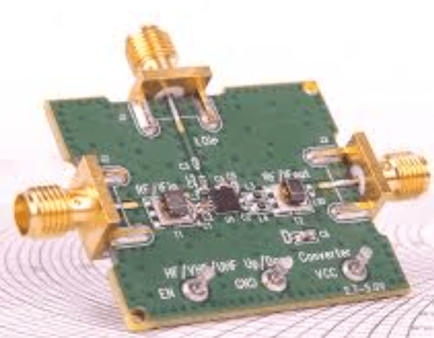
2.1 Improper Component Placement
Poor component placement can lead to signal integrity issues, thermal problems, and manufacturing difficulties. Common errors include placing sensitive analog components too close to digital noise sources or positioning components in ways that complicate routing.
How to avoid: Group components by function, consider signal flow, and plan for thermal management during placement. Always review placement for manufacturability.
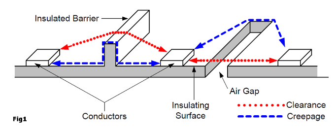
2.2 Insufficient Clearance and Creepage
Failing to maintain proper clearance (air gap) and creepage (surface distance) between conductors can lead to short circuits or compliance issues with safety standards.
How to avoid: Understand the relevant safety standards for your application and configure your DRC (Design Rule Check) settings accordingly. Pay special attention to high-voltage areas.
2.3 Via Mistakes
Common via-related errors include using vias that are too small for the current, placing vias in pads without proper consideration, and not providing enough via stitching in ground planes.
How to avoid: Calculate via sizes based on current requirements. Use tented vias or via-in-pad with plating when necessary. Implement via stitching around high-frequency components.
3. Routing Errors
3.1 Signal Integrity Issues
Poor routing practices can lead to signal integrity problems like crosstalk, reflections, and EMI. Common mistakes include long parallel runs of sensitive signals, improper termination, and ignoring impedance control requirements.
How to avoid: Route critical signals first with appropriate spacing. Use impedance calculation tools and follow length-matching requirements for differential pairs and high-speed signals.
3.2 Power Distribution Problems
Inadequate power distribution manifests as voltage drops, excessive noise, or even complete circuit failure. Designers often underestimate the need for proper power plane design and decoupling capacitor placement.
How to avoid: Calculate power requirements for all components. Use solid power planes where possible and implement a proper decoupling capacitor strategy with capacitors placed close to power pins.
3.3 Thermal Management Oversights
Failing to consider heat dissipation can lead to premature component failure or performance degradation. Common errors include insufficient copper for high-current traces, poor thermal relief design, and inadequate spacing between heat-generating components.
How to avoid: Identify high-power components early in the design process. Use thermal simulation tools when necessary and follow manufacturer recommendations for thermal pads and heatsinks.
4. Design for Manufacturing (DFM) Errors
4.1 Violating Fabrication Capabilities
Designing features beyond the manufacturer’s capabilities (like too small drill sizes or tight tolerances) leads to increased costs or rejected boards.
How to avoid: Always obtain and follow the manufacturer’s design guidelines before starting the layout. Include these specifications in your design rules.
4.2 Solder Mask and Silkscreen Issues
Poor solder mask design can cause solder bridges, while unclear silkscreen can complicate assembly and debugging. Common mistakes include missing solder mask between fine-pitch components and overcrowded silkscreen markings.
How to avoid: Review solder mask coverage, especially in tight areas. Keep silkscreen legible and use it to mark component orientation and critical test points.
4.3 Incorrect Panelization
Improper panelization can lead to manufacturing difficulties or board breakage during depanelization. Designers often forget to include fiducials, tooling holes, or breakaway tabs.
How to avoid: Consult with your manufacturer about panelization requirements early in the design process. Include all necessary tooling features in your design.
5. Documentation and Communication Errors
5.1 Incomplete or Inaccurate Documentation
Missing or incorrect documentation (assembly drawings, BOM, etc.) causes delays and assembly mistakes. Common issues include wrong part numbers, missing polarity markings, or unclear assembly instructions.
How to avoid: Implement a documentation checklist and review process. Use automated tools to generate BOMs from the design data when possible.
5.2 Version Control Problems
Working with wrong file versions or failing to properly document changes can lead to costly mistakes going unnoticed until late in the process.
How to avoid: Implement a strict version control system with clear naming conventions and change logs. Consider using dedicated version control software for hardware projects.
5.3 Lack of Design Review
Skipping design reviews to save time often results in overlooked errors that are more expensive to fix later.
How to avoid: Schedule formal design reviews at key milestones. Use checklist-based reviews and involve team members with different perspectives.
6. Testing and Verification Oversights
6.1 Missing Test Points
Failing to include adequate test points makes debugging and verification difficult, potentially hiding problems until final system integration.
How to avoid: Identify critical signals that need testing early in the design. Include test points for power, ground, clocks, and control signals.
6.2 Ignoring Design Rule Checks (DRC)
Many designers run DRC but then ignore or override important errors, especially when working under tight deadlines.
How to avoid: Treat all DRC errors as serious issues. Document and justify any intentional violations in the design notes.
6.3 Inadequate Design Verification
Relying solely on DRC without additional verification can miss functional problems that aren’t covered by basic design rules.
How to avoid: Perform signal integrity analysis, power distribution network analysis, and thermal analysis where appropriate. Build and test prototypes when possible.
Conclusion
PCB design is a complex process with many opportunities for errors, but most common mistakes can be avoided with careful planning, adherence to best practices, and thorough verification processes. By understanding these common pitfalls and implementing systematic approaches to prevent them, designers can significantly improve their success rate and reduce costly rework.
The key to successful PCB design lies in attention to detail, comprehensive verification at every stage, and learning from past mistakes. Establishing and following standardized design processes, maintaining well-organized component libraries, and fostering a culture of thorough design review will go a long way in minimizing errors in your PCB design work.
Remember that every mistake caught during the design phase saves significant time and money that would otherwise be spent on rework or worse—failed products in the field. Invest in prevention through careful design practices, and your PCB designs will be more reliable, manufacturable, and successful.