Common PCB Defects: Causes, Identification, and Solutions
Introduction to PCB Quality Issues
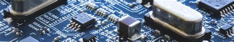
Printed Circuit Boards (PCBs) form the foundation of nearly all modern electronic devices, from smartphones to industrial control systems. As electronic products become more complex and miniaturized, the quality requirements for PCBs have become increasingly stringent. Even minor defects in a PCB can lead to product failure, reduced reliability, or complete system malfunction.
Understanding common PCB defects is essential for manufacturers, quality control professionals, and electronics engineers. This comprehensive guide examines the most prevalent PCB manufacturing and assembly defects, their root causes, methods for identification, and potential solutions to prevent these issues in production.
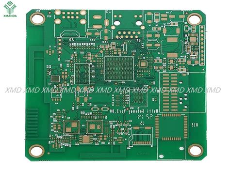
1. Manufacturing Defects in Bare PCBs
1.1 Copper Trace Issues
Open Circuits: One of the most critical defects occurs when the conductive path is broken, preventing current flow. This can result from:
- Under-etching or over-etching during manufacturing
- Mechanical stress causing trace fractures
- Improper handling leading to physical damage
Short Circuits: Unintended connections between traces create short circuits, often caused by:
- Insufficient spacing between traces (design violation)
- Solder bridging during assembly
- Conductive debris contamination
- Copper over-etching leading to “whiskers”
Inconsistent Trace Width: Variations in trace width affect impedance and current-carrying capacity:
- Over-etching reduces trace width
- Under-etching leaves excess copper
- Improper photoresist application
1.2 Substrate and Laminate Problems
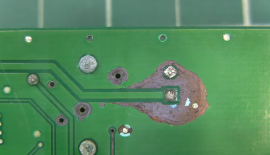
Delamination: Separation of PCB layers due to:
- Moisture absorption before soldering
- Excessive thermal stress during assembly
- Poor adhesive quality in laminate materials
Warping and Twisting: Board deformation caused by:
- Uneven copper distribution creating mechanical stress
- Improper cooling after high-temperature processes
- Inconsistent material properties across layers
Voiding in Plated Through Holes (PTH): Incomplete copper plating in vias and holes:
- Inadequate electroplating process
- Poor hole preparation (drilling debris)
- Solution contamination in plating baths
1.3 Solder Mask Defects
Incomplete Coverage: Areas without proper solder mask protection:
- Improper application technique
- Contamination preventing adhesion
- Insufficient curing
Misregistration: Solder mask misaligned with underlying copper:
- Alignment errors during printing
- Dimensional instability of substrate
- Thermal expansion mismatches
Pinholes and Thin Spots: Small defects in solder mask coverage:
- Dust or debris during application
- Air bubbles in solder mask material
- Inadequate thickness
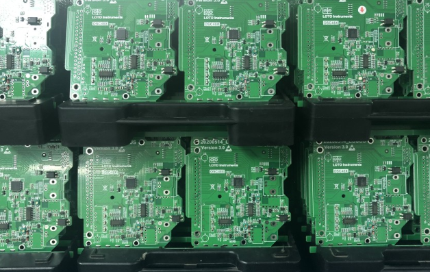
2. Assembly-Related PCB Defects
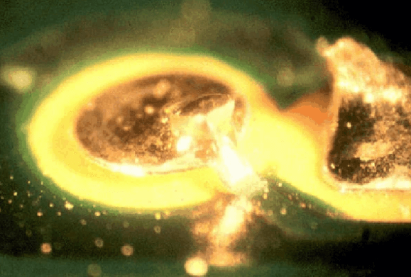
2.1 Soldering Problems
Cold Solder Joints: Characterized by dull, grainy appearance:
- Insufficient heat during soldering
- Contaminated surfaces
- Improper flux application
- Premature movement during cooling
Solder Bridging: Unwanted connections between pads/pins:
- Excessive solder paste application
- Incorrect stencil design
- Component placement inaccuracy
- Insufficient solder mask between pads
Tombstoning: Component lifts on one end during reflow:
- Uneven heating during reflow
- Mismatched pad sizes for two-terminal components
- Imbalanced surface tension forces
2.2 Component Placement Issues
Misalignment: Components not properly positioned:
- Pick-and-place machine calibration errors
- Inaccurate fiducial recognition
- Board support issues during placement
Missing Components: Parts absent from assembly:
- Feeder problems in placement machines
- Vacuum nozzle failures
- Incorrect bill of materials (BOM)
Reverse Polarity: Polarized components installed backwards:
- Inadequate orientation marking
- CAD library errors
- Operator error in manual assembly
2.3 BGA and QFN Package Defects
Head-in-Pillow: Solder ball doesn’t fully merge with paste:
- Warpage during reflow
- Oxidation on solder balls
- Insufficient reflow temperature
Non-Wet Opens: Solder fails to bond with pad:
- Contaminated surfaces
- Insufficient flux activity
- Oxidation of surfaces
Voiding in Solder Joints: Gas pockets within solder:
- Outgassing from flux or contaminants
- Improper reflow profile
- Poor paste quality
3. Environmental and Reliability Defects
3.1 Electrochemical Migration
Dendritic Growth: Metal filaments causing shorts:
- Ionic contamination on surface
- Moisture presence
- Applied voltage bias
Conductive Anodic Filament (CAF): Growth along glass fibers:
- High humidity environments
- DC voltage potential
- Poor laminate quality
3.2 Thermal Stress Defects
Pad Cratering: Fractures under component terminations:
- CTE mismatch between materials
- Mechanical shock or vibration
- Brittle solder intermetallics
Barrel Cracking in Vias: Fractures in plated through holes:
- Thermal cycling stress
- Poor copper plating quality
- Excessive z-axis expansion
3.3 Mechanical Stress Defects
Cracked Components: Ceramic parts fracture:
- Board flexure during handling
- Excessive mounting pressure
- Thermal shock
Trace Fractures: Broken copper conductors:
- Vibration-induced fatigue
- Mechanical impact
- Poor bend radius in flexible circuits
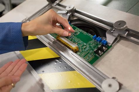
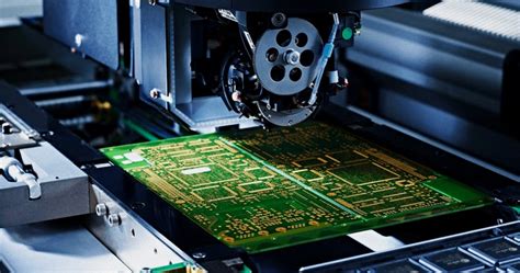
4. Inspection and Detection Methods
4.1 Visual Inspection
- Manual inspection under magnification
- Optical comparators for pattern verification
- Microscopic examination of solder joints
4.2 Automated Optical Inspection (AOI)
- 2D and 3D imaging systems
- Pattern recognition algorithms
- Solder joint quality assessment
4.3 X-Ray Inspection
- Internal structure visualization
- BGA and QFN joint analysis
- Void detection and measurement
4.4 Electrical Testing
- Flying probe testing for opens/shorts
- In-circuit testing (ICT) for component verification
- Boundary scan testing for digital circuits
4.5 Environmental Stress Testing
- Thermal cycling to reveal latent defects
- Vibration testing for mechanical robustness
- Humidity testing for moisture sensitivity
5. Prevention and Quality Control Strategies
5.1 Design for Manufacturing (DFM)
- Adherence to design rules and constraints
- Proper spacing and clearances
- Thermal relief considerations
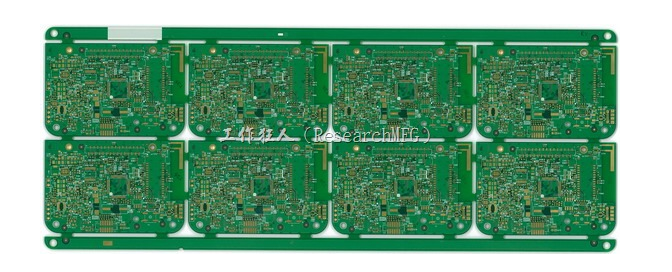
- Panelization and fiducial design
5.2 Process Control
- Solder paste printing optimization
- Reflow profile development
- Cleanliness and contamination control
- Moisture sensitive component handling
5.3 Material Selection
- High-quality laminate materials
- Appropriate solder mask formulations
- Reliable solder paste composition
- Compatible flux chemistry
5.4 Supplier Qualification
- Rigorous PCB fabricator evaluation
- Component supplier audits
- Material certification requirements
- Process capability analysis
Conclusion
PCB defects can originate from multiple sources throughout the design, fabrication, and assembly processes. Understanding these potential failure modes enables manufacturers to implement appropriate preventive measures and detection methods. As PCB technology continues to advance with higher densities, finer pitches, and more complex architectures, maintaining high quality standards becomes both more challenging and more critical.
Effective quality management requires a comprehensive approach combining robust design practices, controlled manufacturing processes, thorough inspection methodologies, and continuous improvement initiatives. By addressing PCB defects systematically at each stage of production, manufacturers can significantly improve product reliability, reduce warranty costs, and enhance customer satisfaction in today’s competitive electronics marketplace.