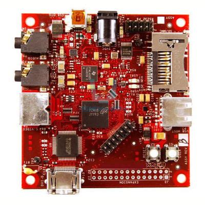
Common PCB Design Mistakes
When developing electronic products,PCBs are used to connect electronic component to each other.Therefore,even small design errors can lead to complete failure.While new design tools have reduced the cost of pcb manufacturing over the past few years,poor PCB design can also increase costs.Therefore,PCB designer must avoid these PCB design mistakes.
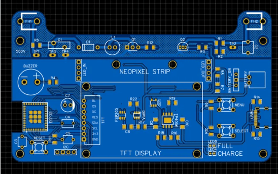
Incorrect PCB component landing patterns
PCB design software tools include libraries of common electronic component from these libraries.Using components from these libraries is convenient,but due to PCB design rules,problem arise when you want to use component not included in the libraries.When using components not in the library,engineers must manually draw the schematic symbols and landing patterns are common,as a single millimeter difference in pin-to -pin spacing can prevent the component from soldering correctly to the board.
Wireless antenna layout is a PCB design mistake
For wireless products ,antenna PCB layout is extremely important.Impedance matching is essential to maximize power transfer between the transceiver and antenna.To achieve this ,two key consideration are a suitable microstrip connection between the antenna and the transceiver.This step is often where most PCB designers make mistakes,so they must pay close attention when performing this step.
Decoupling Capacitor Placement on the PCB
Critical circuit board component like decoupling capacitors require a clean and stable voltage source,so they are placed on thr power rails.However, for decoupling capacitors to be most effective ,they must be placed as close as possible to the pins requiring the stable voltage.Therefore,the power supply trace from the power supply must be routed so that they first connect to the decoupling capacitors and then to the pins requiring the stable voltage.Placing the output capacitors of the power regulator as close as possible to the regulator’s output pins is also crucial,as this is necessary for optimizing stability and improving transient response.
Avoid Insufficient Power Trace Width
Trace width depends on several factors,such as whether the trace is internal or external and the thickness(copper weight)of the trace.If the pcb trace carries more than 500mA of current,the minimum allowable width may not be sufficient.Trace thickness depends on the amount of copper used in the layer.Most PCB manufacturers allow a copper weight of around 0.5 ounces per square foot.
PCB Copper Thickness
It is recommended to select a finished copper thickness of 1 to 2 ounces per square foot,but designer often prefer a finished copper thickness of 1 ounce.This can cause problems because it may not provide sufficient plating volume in through-holes and vias.
Choosing the Wrong Design Tools for PCB Design
Choosing the right tools for PCB design is a very important and fundamental step.It is recommended to select the tools that best suit the PCB design requirement,as choosing the wrong tools can lead to design delays and increased manufacturing costs.
Tombstone Effect in PCBs
Tombstone effect can significantly affect pcb yield and significantly increase production costs.When soldering small passive surface-mount components to a PCB using the reflow process.it is common to see one end lift up,creating a “tombstone effect”Tombstone effect can be caused by an incorrect landing pattern or uneven heat dissipation from the pad.Using Design for Functionality(DFM) checks can reduce tomstone effect can be caused by an incorrect landing pattern or uneven heat disspation from the pad.Using Design for Functionality checks can reduce tombstone effects.
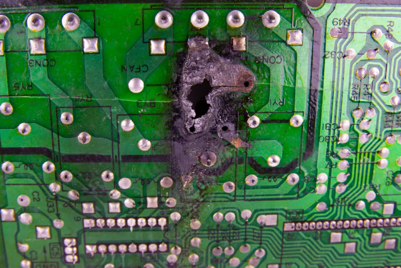
Missing Solder Mask Between Pads
It is common to find no solder mask between the pins of tightly packaged, small, lead-clamped devices. When these thin pins are connected to the PCB during assembly, the lack of this solder mask can lead to solder bridges.
Lack of Design Review
Design review is a very important process in PCB design. It involves reviewing design features, PCB functionality, and circuit interconnections. It’s beneficial to review your design so you can avoid design errors.
Not Backing Up Project Files
Different software is used when creating successful PCBs. Due to the software’s high flexibility and speed, some data can be easily lost. To avoid this problem, it’s a good practice to save data frequently. Creating save points ensures that even if one save point is damaged, the others will still function properly.