Common PCB Layout Traps and How to Avoid Them
Introduction
Printed Circuit Board (PCB) design is both an art and a science that requires careful consideration of numerous factors to ensure optimal performance, reliability, and manufacturability. Even experienced engineers can fall into common layout traps that may lead to signal integrity issues, electromagnetic interference (EMI) problems, thermal challenges, or manufacturing defects. This article explores the most prevalent PCB layout pitfalls encountered in modern electronics design and provides practical solutions to avoid them.
1. Improper Power Distribution Network (PDN) Design
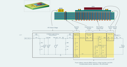
The Decoupling Dilemma
One of the most frequent mistakes in PCB layout is inadequate power distribution network design. Many designers underestimate the importance of proper decoupling capacitor placement and selection, leading to power integrity issues that manifest as random resets, signal integrity problems, or excessive EMI.
Common traps include:
- Placing decoupling capacitors too far from IC power pins
- Using insufficient quantity or wrong values of decoupling capacitors
- Neglecting to account for capacitor self-resonant frequencies
- Creating long power traces before reaching decoupling capacitors
Best practices:
- Place the smallest value decoupling capacitor closest to the power pin
- Use multiple capacitor values in parallel to cover a broad frequency range
- Keep power and ground return paths as short as possible
- Consider using power planes instead of traces for high-current devices
2. Signal Integrity Oversights
Transmission Line Neglect
With increasing signal speeds, many designers fail to properly account for transmission line effects, leading to signal reflections, crosstalk, and timing errors.
Common signal integrity traps:
- Not implementing proper impedance control for high-speed signals
- Ignoring return current paths for critical signals
- Creating unnecessarily long parallel trace runs that increase crosstalk
- Failing to maintain consistent impedance at transitions (vias, connectors)
Solutions:
- Calculate and maintain controlled impedance for critical traces
- Provide uninterrupted reference planes beneath high-speed signals
- Use differential pair routing for sensitive signals
- Implement proper termination strategies (series, parallel, or AC termination)
3. Grounding Pitfalls
The Myth of the “Perfect Ground”
Grounding issues account for a significant percentage of PCB problems, yet many designers treat ground as an afterthought rather than a critical system component.
Common grounding traps:
- Creating ground loops by using multiple return paths
- Implementing “star ground” inappropriately for mixed-signal designs
- Splitting ground planes unnecessarily
- Failing to consider high-frequency return currents
Proper grounding techniques:
- Use a solid ground plane whenever possible
- For mixed-signal designs, partition the ground plane by function rather than physically splitting it
- Provide low-impedance return paths for high-frequency currents
- Be mindful of slotting in ground planes that can disrupt return paths
4. Thermal Management Mistakes
Overlooking Heat Dissipation Requirements
As component densities increase, thermal considerations become more critical, yet many layouts fail to properly address heat dissipation needs.
Thermal layout traps:
- Placing heat-sensitive components near high-power devices
- Not providing adequate copper area for heat dissipation
- Ignoring thermal relief requirements for soldering
- Failing to consider airflow in the final enclosure
Thermal management solutions:
- Perform thermal analysis during the layout phase
- Use thermal vias under hot components to transfer heat to other layers
- Provide adequate copper pours connected to component thermal pads
- Consider the placement of components in relation to expected airflow
5. Manufacturing Oversights
Designing Without Considering Fabrication Realities
Many PCB designs are theoretically sound but run into problems during manufacturing due to overlooked fabrication constraints.
Common manufacturing traps:
- Specifying unrealistic trace/space requirements
- Creating acid traps with acute angles in traces
- Placing components too close to board edges
- Not accounting for solder mask expansion
- Ignoring test point accessibility
Design for Manufacturing (DFM) tips:
- Consult with your PCB manufacturer early about their capabilities
- Avoid acute angles in copper features
- Provide adequate spacing between components and board edges
- Include test points for critical signals
- Consider panelization requirements for small boards
6. Component Placement Errors
The Domino Effect of Poor Placement
Component placement sets the stage for the entire layout, and early mistakes can lead to cascading problems throughout the design process.
Placement traps:
- Not grouping related components together
- Placing connectors in inconvenient locations
- Ignoring mechanical constraints
- Failing to consider rework accessibility
- Not accounting for component height restrictions
Optimal placement strategies:
- Start with critical components (connectors, processors, etc.)
- Group functional blocks together logically
- Consider signal flow through the board
- Account for mechanical constraints early
- Leave space for rework and debugging access

7. Via Misuse and Abuse
The Hidden Costs of Poor Via Implementation
Vias are essential for multilayer boards but are often implemented poorly, creating reliability and signal integrity issues.
Via-related traps:
- Using too few vias for high-current paths
- Placing vias in pad without proper consideration
- Creating via stubs in high-speed signals
- Not accounting for via impedance discontinuities
Proper via implementation:
- Use multiple vias for high-current connections
- Consider via-in-pad carefully (may require filling)
- Use back-drilling for critical high-speed signals
- Account for via impedance in high-speed designs
8. EMI/EMC Oversights
Unintentional Antenna Design
Many PCB layouts inadvertently create excellent antennas for electromagnetic interference, failing to meet EMC requirements.
EMI traps:
- Creating large current loops
- Having unbalanced differential pairs
- Leaving unterminated transmission lines
- Not providing proper shielding for sensitive circuits
EMI reduction techniques:
- Minimize current loop areas
- Maintain symmetry in differential pairs
- Implement proper filtering at cable interfaces
- Consider shielding strategies for sensitive circuits
9. Documentation Deficiencies
The Forgotten Art of Clear Documentation
Even the best PCB designs can be undermined by poor documentation, leading to manufacturing errors and debugging difficulties.
Documentation traps:
- Incomplete or unclear layer stackup information
- Missing or ambiguous fabrication notes
- Poor component designators and silkscreen placement
- Lack of version control information
Documentation best practices:
- Provide complete layer stackup details
- Include clear fabrication and assembly notes
- Place useful information on silkscreen layers
- Implement a robust version control system
Conclusion
PCB layout is a complex undertaking with numerous potential pitfalls that can affect performance, reliability, and manufacturability. By being aware of these common traps—from power distribution mistakes to documentation deficiencies—designers can proactively avoid them in their layouts. The key to successful PCB design lies in careful planning, attention to detail, and consideration of all aspects from electrical performance to mechanical constraints to manufacturing requirements.
Remember that every design is unique, and what works for one project may not be appropriate for another. Continuously educating yourself about current best practices, consulting with manufacturing partners early in the design process, and learning from past mistakes will help you create robust, reliable PCB layouts that perform as intended in their final application.