Common problems and improvement measures for PCB design
With the continuous development of modern electronic technology, the requirements for hardware design are getting higher and higher. As the basis of hardware design, PCB design occupies a vital position in the entire production process of electronic products. However, in the actual PCB design process, some common problems often occur due to various reasons. This article will introduce the common problems in PCB design and possible improvement measures in detail.
1.Inconsistent symbol library
In the early stage of PCB design, schematic design is usually required, and the symbol library is the basis of schematic design. The common problem of inconsistent symbol libraries refers to the use of different symbol libraries in a project, which will cause a lot of trouble for later projects.
Solution:
- Establish a unified symbol library within the company to facilitate sharing in different projects.
- In the early stage of PCB design, check each symbol library to avoid conflicts between different symbol libraries.
- High routing cost
In PCB design, the complexity of the circuit will affect the circuit layout and routing. If the routing is unreasonable, it may lead to high routing costs and affect the reliability and stability of the circuit.
Solution:
- When laying out the circuit, the simplicity and reliability of the circuit structure should be given priority, and the number of traces should be reduced as much as possible to reduce the trace cost.
- For circuits that require a large number of traces, consider using a multi-layer printed circuit board design method, so that the trace cost can be reduced through wiring.
- Power supply noise interference
In PCB design, power supply noise interference is a common problem. This noise interference may have an adverse effect on the stability and reliability of the circuit, and even cause the circuit to fail.
Solution:
- When designing PCB, the intersection of power lines and signal lines should be avoided as much as possible to reduce power supply noise interference.
- For applications that need to ensure circuit stability and reliability, multiple power supply filters can be used to reduce power supply noise interference.
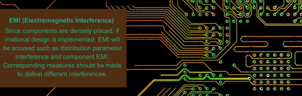
- Electromagnetic compatibility issues
Electromagnetic compatibility issues are also a common problem in PCB design. Electromagnetic interference may cause noise interference, signal truncation, communication failure and other problems.
Solution:
- When designing PCB, the correct electromagnetic shielding materials and methods should be used to reduce electromagnetic interference.
- Through appropriate electromagnetic compatibility tests, determine whether the circuit meets the relevant electromagnetic compatibility standards.
V. Mixing discrete devices with integrated devices
In PCB design, some designers will mix discrete devices with integrated devices, which may increase the complexity of the circuit and may also reduce the sensitivity and reliability of the circuit.
Solution:
- Designers should use integrated devices as much as possible, which can reduce the complexity and reliability of the circuit.
- When using discrete devices, attention should be paid to the matching of parameters such as current and voltage to fully ensure the stability and reliability of the circuit.
VI. Package and layout mismatch
In PCB design, package and layout mismatch is a common problem. This may cause problems such as circuit abnormalities or inconvenience in modification.
Solution:
- Designers should verify the package and establish a tool library to ensure the matching of the package and layout.
- Before PCB design, the package should be carefully checked and converted to ensure its correctness and consistency.
- Unreasonable layer planning
In multi-layer PCB design, unreasonable layer planning will lead to problems such as circuit parasitic capacitance and electromagnetic interference, thereby affecting the stability and reliability of the circuit.
Solution:
- In multi-layer PCB design, layer planning should be comprehensively considered from the aspects of electromagnetic compatibility, signal integrity, power supply sequence, etc.
- Designers should try to avoid inter-layer crossing, signal routing layer and power routing layer, layer sequence, etc., to ensure the rationality of layer planning.
- Failure to consider the impact of high-speed signals
In the transmission of high-speed signals, slight changes and capacitance differences on the circuit board may cause extremely significant magical signal distortion.
Solution:
- Avoid unnecessary line length and wiring corners to reduce electromagnetic interference that causes signal distortion.
- Use microstrip and coaxial wiring as much as possible to reduce signal distortion.
In summary, common problems in PCB design include inconsistent symbol libraries, high routing costs, power supply noise interference, electromagnetic compatibility issues, mixed use of discrete devices and integrated devices, mismatch between packaging and layout, unreasonable layer planning, and failure to consider the impact of high-speed signals. When solving these problems, different aspects should be considered, such as the unification of symbol libraries, simplicity and reliability of circuit layout, stability and reliability of circuits, etc. Only by adopting scientific solutions can the quality of PCB design be effectively guaranteed, making electronic products more stable and reliable.