Common Problems and Solutions in RF Integrated Circuit Design
RF (RF) PCB design has many uncertainties in the currently published theories and is often described as a “black art”. Generally speaking, for circuits below the microwave frequency band (including low-frequency and low-frequency digital circuits), careful planning under the premise of fully mastering various design principles is the guarantee of a one-time successful design. For PC-type digital circuits above the microwave frequency band and high frequency, 2~3 versions of PCB are required to ensure the quality of the circuit. For RF circuits above the microwave frequency band, more versions of PCB design are often required and continuously improved, and this is based on considerable experience. This shows the difficulty of RF electrical design.
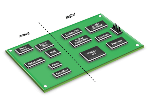
Interference between digital circuit modules and analog circuit modules
If the analog circuit (RF) and the digital circuit work separately, they may work well separately. However, once the two are placed on the same circuit board and work together using the same power supply, the entire system is likely to be unstable. This is mainly because digital signals frequently swing between the ground and the positive power supply (>3 V), and the cycle is particularly short, often in the nanosecond level. Due to the large amplitude and short switching time, these digital signals contain a large amount of high-frequency components that are independent of the switching frequency. In the analog part, the signal transmitted from the wireless tuning loop to the receiving part of the wireless device is generally less than 1μV. Therefore, the difference between the digital signal and the RF signal can reach 120dB. Obviously, if the digital signal and the RF signal cannot be separated well, the weak RF signal may be destroyed, so that the working performance of the wireless device will deteriorate or even fail to work at all.
Noise interference of power supply
RF circuits are very sensitive to power supply noise, especially to glitch voltage and other high-frequency harmonics. Microcontrollers will suddenly absorb most of the current for a short time in each internal clock cycle. This is because modern microcontrollers are manufactured using CMOS technology. Therefore, assuming that a microcontroller runs at an internal clock frequency of 1MHz, it will extract current from the power supply at this frequency. If proper power supply decoupling is not taken, voltage glitches on the power supply line will inevitably occur. If these voltage glitches reach the power pins of the RF part of the circuit, they may cause work failure in severe cases.
Unreasonable ground wire
If the ground wire of the RF circuit is not handled properly, some strange phenomena may occur. For digital circuit design, most digital circuit functions perform well even without a ground plane. In the RF band, even a very short ground line will act like an inductor. Roughly calculated, the inductance per millimeter length is about 1nH, and the inductance of a 10mmPCB line at 433MHz is about 27Ω. If a ground plane is not used, most ground lines will be long and the circuit will not have the designed characteristics.
Radiated interference of antennas to other analog circuit parts
In PCB circuit design, there are usually other analog circuits on the board. For example, many circuits have analog/digital converters (ADCs) or digital/analog converters (DACs). The high-frequency signal emitted by the antenna of the RF transmitter may reach the analog input of the ADC. Because any circuit line may emit or receive RF signals like an antenna. If the processing of the ADC input is not reasonable, the RF signal may self-excite in the ESD diode of the ADC input, causing ADC deviation.
RF circuit design principles and solutions
RF layout concept
When designing RF layout, the following general principles must be met first:
(1) Isolate the high-power RF amplifier (HPA) and the low-noise amplifier (LNA) as much as possible. Simply put, keep the high-power RF transmitting circuit away from the low-power RF receiving circuit;
(2) Ensure that there is at least one whole ground in the high-power area of the PCB board, preferably without vias. Of course, the larger the copper foil area, the better;
(3) Circuit and power decoupling are also extremely important;
(4) RF output usually needs to be away from RF input;
(5) Sensitive analog signals should be as far away from high-speed digital signals and RF signals as possible.
Physical partition and electrical partition design principles
Design partitions can be decomposed into physical partitions and electrical partitions. Physical partitions mainly involve component layout, direction and shielding; electrical partitions can be further decomposed into power distribution, RF routing, sensitive circuits and signals, and grounding.
Physical partition principles
(1) Component location layout principles. Component layout is the key to achieving an excellent RF design. The most effective technique is to first fix the components on the RF path and adjust their direction so as to minimize the length of the RF path, keep the input away from the output, and separate the high-power circuit and the low-power circuit as far as possible.
(2) PCB stacking design principles. The most effective circuit board stacking method is to arrange the main ground plane (main ground) on the second layer under the surface layer and arrange the RF line on the surface layer as much as possible. Minimize the size of the vias on the RF path, which can not only reduce the path inductance, but also reduce the number of cold solder joints on the main ground and reduce the chance of RF energy leaking to other areas in the stacked board.
(3) RF devices and their RF wiring layout principles. In physical space, linear circuits such as multi-stage amplifiers are usually sufficient to isolate multiple RF areas from each other, but duplexers, mixers, and intermediate frequency amplifiers/mixers always have multiple RF/IF signals interfering with each other, so this effect must be carefully minimized. RF and IF traces should be crossed as much as possible, and a ground plane should be placed between them as much as possible. Correct RF paths are very important to the performance of the entire PCB, which is why component layout usually takes up most of the time in cell phone PCB design.
(4) Design principles for reducing interference coupling between high/low power devices. On a cell phone PCB, it is usually possible to reduce noise by placing the amplifier circuit on one side of the PCB and the high power amplifier on the other side, and finally connect them to the antenna on the RF and baseband processor sides on the same side through a duplexer. Skills are required to ensure that the through holes do not transfer RF energy from one side of the board to the other side. A common technique is to use blind holes on both sides. The adverse effects of through holes can be minimized by arranging through holes in areas on both sides of the PCB that are not affected by RF interference.
Electrical partitioning principles
(1) Power transmission principles. The DC current of most circuits in cell phones is quite small, so the wiring width is usually not a problem. However, a separate high current line as wide as possible must be set for the power supply of the high power amplifier to minimize the transmission voltage drop. In order to avoid too much current loss, multiple through holes are required to transfer current from one layer to another.
(2) Power supply decoupling of high-power devices. If the power supply pin of the high-power amplifier cannot be adequately decoupled, high-power noise will radiate to the entire board and cause multiple problems. The grounding of the high-power amplifier is quite critical and often requires a metal shielding cover.
(3) RF input/output isolation principle. In most cases, it is also critical to ensure that the RF output is far away from the RF input. This also applies to amplifiers, buffers and filters. In the worst case, if the outputs of amplifiers and buffers are fed back to their inputs with appropriate phase and amplitude, they may produce self-oscillation. In the best case, they will be able to operate stably under any temperature and voltage conditions. In fact, they may become unstable and add noise and intermodulation signals to the RF signal.
(4) Filter input/output isolation principle. If the RF signal line has to loop back from the input of the filter to the output, then this may seriously damage the bandpass characteristics of the filter. In order to isolate the input and output well, first a circle of ground must be arranged around the filter, and secondly a ground must be arranged in the lower area of the filter and connected to the main ground surrounding the filter. It is also a good idea to keep the signal lines that need to pass through the filter as far away from the filter pins as possible. In addition, the grounding of various places on the entire board must be very careful, otherwise an undesirable coupling channel may be introduced unconsciously.
(5) Isolation of digital circuits and analog circuits. In all PCB designs, it is a general principle to keep digital circuits as far away from analog circuits as possible, which also applies to RF PCB design. The common analog ground and the ground used to shield and separate signal lines are usually equally important. Design changes caused by negligence may cause the design that is about to be completed to be torn down and re-done. Similarly, RF lines should be kept away from analog lines and some very critical digital signals. All RF traces, pads and components should be filled with as much ground copper as possible and connected to the main ground as much as possible. If the RF trace must pass through the signal line, try to arrange a layer of ground connected to the main ground between them along the RF trace. If this is not possible, make sure they are cross-crossed, which can minimize capacitive coupling. At the same time, try to lay more ground around each RF trace and connect them to the main ground. Additionally, minimizing the distance between parallel RF traces can minimize inductive coupling.