Common Problems in PCB Assembly and How to Solve Them
Printed Circuit Board (PCB) assembly is a complex process that involves multiple steps, from design and component placement to soldering and testing. Despite advancements in technology, various issues can arise during PCB assembly, leading to defects, failures, or reduced performance. This article explores the most common problems encountered in PCB assembly, their causes, and potential solutions to ensure high-quality production.
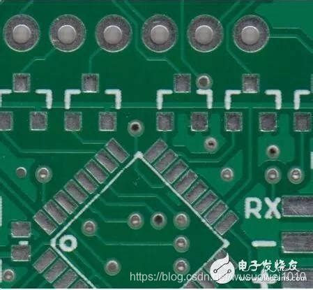
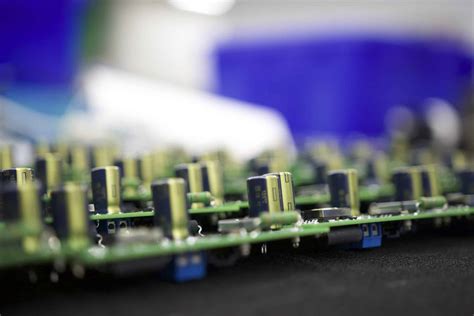
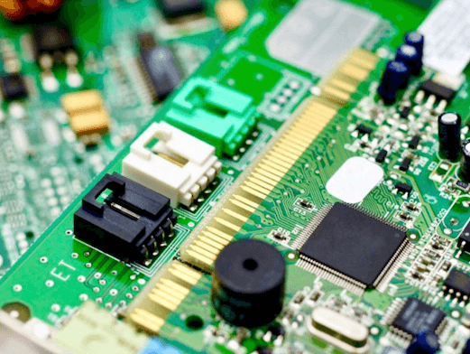
1. Soldering Defects
Soldering is a critical step in PCB assembly, and defects in this process can lead to poor electrical connections or complete circuit failure. Common soldering issues include:
a. Cold Solder Joints
A cold solder joint occurs when the solder does not melt properly, resulting in a weak or incomplete connection. This can happen due to insufficient heat, contamination, or improper flux application.
Solution:
- Ensure proper soldering temperature and time.
- Use high-quality flux to improve wetting.
- Inspect solder joints visually or with X-ray for quality assurance.
b. Solder Bridging
Solder bridging happens when excess solder creates an unintended connection between two adjacent pins or traces, causing short circuits.
Solution:
- Optimize solder paste application using stencil printing.
- Use solder masks to prevent excess solder flow.
- Implement automated optical inspection (AOI) to detect bridges early.
c. Tombstoning
Tombstoning occurs when a surface-mount component stands vertically on one end due to uneven solder paste application or thermal imbalance.
Solution:
- Ensure even solder paste deposition.
- Balance component pad sizes and thermal profiles.
- Use reflow ovens with controlled heating zones.
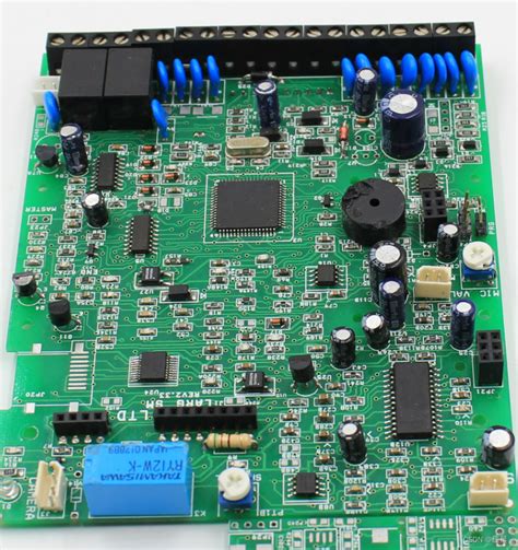
2. Component Placement Issues
Incorrect component placement can lead to misalignment, poor connections, or non-functional boards. Common problems include:
a. Misaligned Components
Misalignment happens when components are not placed accurately on their designated pads, leading to poor soldering or open circuits.
Solution:
- Use high-precision pick-and-place machines.
- Verify component orientation before assembly.
- Implement vision systems for alignment verification.
b. Missing or Wrong Components
Human or machine errors can result in missing components or incorrect part placements.
Solution:
- Use barcode scanning for component verification.
- Conduct pre-assembly checks of the Bill of Materials (BOM).
- Perform post-placement inspections using AOI.
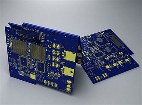
3. PCB Design Flaws
Many assembly issues stem from design errors that affect manufacturability. Common design-related problems include:
a. Insufficient Clearance Between Components
If components are placed too close together, soldering and inspection become difficult, increasing the risk of shorts.
Solution:
- Follow Design for Manufacturability (DFM) guidelines.
- Maintain proper spacing between components.
- Use simulation tools to verify layouts before production.
b. Poor Thermal Management
Inadequate heat dissipation can cause overheating, leading to component failure.
Solution:
- Incorporate thermal vias and heat sinks.
- Optimize copper pour for better heat distribution.
- Select components with appropriate thermal ratings.
4. Contamination and Environmental Factors
Contaminants such as dust, moisture, or chemical residues can affect PCB performance and longevity.
a. Flux Residue Corrosion
Uncleaned flux residues can corrode traces or cause electrical leakage over time.
Solution:
- Use no-clean flux where possible.
- Implement thorough cleaning processes (e.g., ultrasonic cleaning).
- Apply conformal coating for additional protection.
b. Moisture Absorption
Moisture can lead to delamination or “popcorning” (internal cracks in components during reflow).
Solution:
- Store PCBs and components in moisture-controlled environments.
- Pre-bake moisture-sensitive components before assembly.
- Use desiccants in packaging.
5. Electrical and Functional Failures
Even after assembly, PCBs may fail due to electrical issues such as:
a. Open Circuits
Open circuits occur when a trace is broken or a solder joint fails, disrupting current flow.
Solution:
- Perform continuity testing.
- Use high-resolution X-ray inspection for hidden defects.
- Ensure proper trace width and durability in design.
b. Short Circuits
Short circuits can result from solder bridging, damaged insulation, or design errors.
Solution:
- Conduct electrical testing (e.g., flying probe or in-circuit testing).
- Inspect for debris or metal shavings causing shorts.
- Verify PCB layout for unintended connections.
6. Mechanical and Structural Issues
Physical stress can damage PCBs during assembly or operation.
a. Warping or Twisting
Uneven heating or poor material selection can cause PCB warping.
Solution:
- Use high-quality laminate materials.
- Optimize reflow temperature profiles.
- Implement support fixtures during assembly.
b. Pad Lifting
Excessive heat or mechanical stress can detach pads from the PCB.
Solution:
- Control soldering temperature and duration.
- Avoid excessive mechanical force during rework.
- Use reinforced pads for high-stress areas.
Conclusion
PCB assembly involves numerous potential pitfalls, from soldering defects to design flaws and environmental factors. By understanding these common problems and implementing preventive measures—such as DFM guidelines, automated inspections, and proper handling—manufacturers can significantly reduce defects and improve product reliability. Continuous process improvement, employee training, and advanced inspection technologies are key to achieving high-quality PCB assembly.
By addressing these challenges proactively, electronics manufacturers can enhance yield rates, reduce costs, and deliver robust, high-performance PCBs for various applications.