Comparison of single-layer and double-layer boards
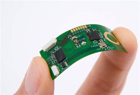
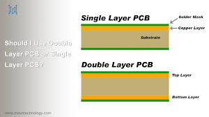
What is a single-sided PCB
Single-sided PCB is the most basic circuit board in the PCB industry. As the name implies, single-sided PCB has wires on one side and plug-in parts on the other side. Single-sided PCB was widely used in various industries in the early days, but because single-sided PCB has high requirements for wiring, each wire must have a separate path and cannot cross; for PCB boards with more wiring, the stability is not enough and the performance is also missing, and it has gradually developed towards double-sided PCB. Therefore, the utilization rate and yield of single-sided PCB are also gradually declining; at present, single-sided PCB is more widely used in power boards.
What is a double-sided PCB
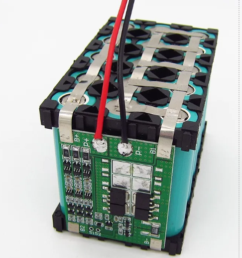
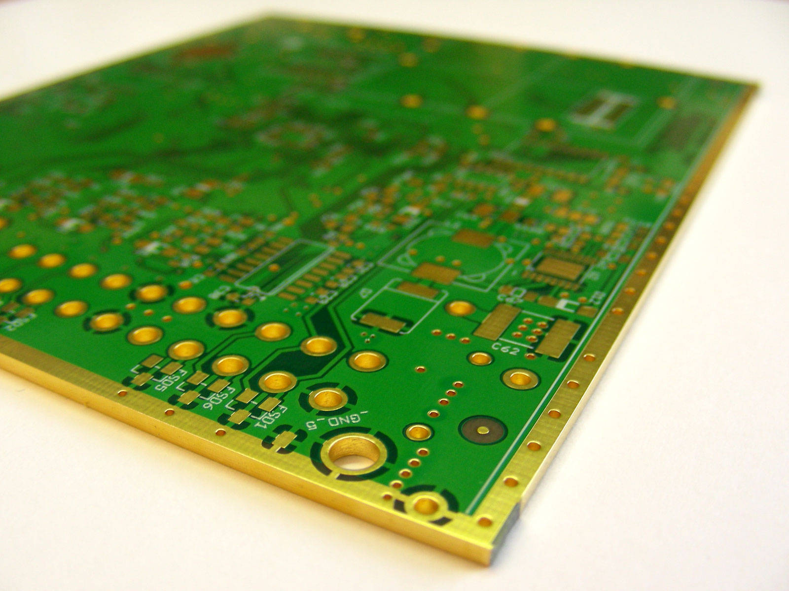
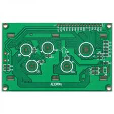
Double-sided PCB is a board with double-sided wiring on the board. An important feature of double-sided PCB is that it has guide holes to connect the wires on both sides into a circuit. The wiring of double-sided PCB can be interlaced with each other, which is the biggest difference from single-sided PCB; double-sided PCB is more suitable for complex circuits and has a wider range of use.
The cost difference between single and double-sided PCB is not much. If there is no special requirement, all industries will give priority to double-sided PCB; after all, the performance and stability of double-sided PCB are better than single-sided PCB.
GET PCB MANUFACTURING AND ASSEMBLY QUOTE NOW!
The difference between single-layer and double-layer PCBs
In the field of printed circuit board (PCB) design and manufacturing, single-layer and double-layer boards are two common choices. They differ significantly in design complexity, manufacturing cost, signal integrity, application areas, wiring density, and heat dissipation performance.
1. Design complexity is an important differentiating factor.
Single-layer boards have only one conductive layer, and the design is relatively simple, suitable for relatively basic circuits.
However, double-layer boards have two conductive layers, allowing more complex circuit designs and higher functional integration. This requires more expertise and experience in the design of double-layer boards.
2. Manufacturing cost
It is also a key differentiating point. Due to the simple structure of single-layer boards, the manufacturing process is relatively simple and the cost is low. In contrast, the manufacturing process of double-layer boards is more complicated and requires additional process steps, such as the production of interlayer connections (vias), which increases the manufacturing cost.
Therefore, in projects with limited budgets, single-layer boards are usually a more economical choice.
3. Signal integrity
Single-layer boards have only one conductive layer, the signal path is longer, and they are susceptible to interference and have poor signal integrity. By adding a conductive layer, double-layer boards can better manage signal paths, reduce interference, and improve signal integrity. This is especially important for high-frequency circuits and applications that require high-precision signal transmission.
4. Application fields
In terms of application fields, single-layer boards and double-layer boards also have different applicable scenarios. Single-layer boards are usually used for simple consumer electronics, household appliances, and some low-cost industrial equipment. Double-layer boards are widely used in more complex electronic devices, such as computer motherboards, communication equipment, and high-end consumer electronics. This is because double-layer boards can support more complex circuit designs and higher functional requirements.
Wiring density is another significant difference. Single-layer boards have only one conductive layer, so the wiring density is limited and it is difficult to support complex circuit designs.
Double-layer boards can significantly increase the wiring density by adding a conductive layer, supporting more complex circuit layouts and more components. This gives double-layer boards a clear advantage in applications that require high-density wiring.
Finally, heat dissipation performance is also a factor that needs to be considered. Single-layer boards have relatively poor heat dissipation performance due to only one conductive layer, which can easily cause circuit overheating.
Double-layer boards can more effectively disperse heat and improve heat dissipation performance by adding a conductive layer. This is especially important for electronic devices that need to operate stably for a long time.
In summary, there are significant differences between single-layer boards and double-layer boards in terms of design complexity, manufacturing cost, signal integrity, application areas, wiring density, and heat dissipation performance. The choice of which type of PCB should be determined based on specific application needs, budget, and technical requirements.
GET PCB AND ASSEMBLY SERVICE QUOTE NOW!
Similarities between single-layer and double-layer boards
Single-layer boards and double-layer boards have similarities in many aspects. First of all, in terms of materials, both usually use the same substrate, such as FR-4, which is a glass fiber reinforced epoxy resin laminate.
FR-4 material is widely used in the manufacture of printed circuit boards (PCBs) due to its excellent mechanical strength and electrical insulation properties.
In addition, copper foil is also a common material for single-layer boards and double-layer boards, which is used to form circuit patterns. Whether it is a single-layer board or a double-layer board, the thickness and quality of the copper foil have an important impact on the performance of the circuit board.
In terms of manufacturing process, single-layer boards and double-layer boards also have many similarities. Both need to go through steps such as drilling, etching, lamination, and surface treatment. Although double-layer boards require an additional lamination step to combine two layers of copper foil during manufacturing, the basic process remains similar.
Etching processes are used to remove excess copper foil and form the desired circuit pattern, while drilling processes are used to create holes for electrical connection points and mounting components. Surface treatments such as tinning or gold plating are used to protect the copper foil and improve soldering performance.
In terms of application areas, both single-layer boards and double-layer boards are widely used in various electronic devices. Single-layer boards are usually used in simple electronic products such as home appliances and toys, while double-layer boards are more commonly used in complex electronic devices such as computers and communication equipment. However, both are widely used in many mid- and low-end electronic products to meet different design needs and cost considerations.
Design rules are also a common point between single-layer boards and double-layer boards. Whether it is a single-layer board or a double-layer board, designers need to follow certain design rules to ensure the reliability and manufacturability of the circuit board.
These rules include minimum line width, minimum spacing, aperture size, and pad size. Compliance with design rules not only helps improve the performance of the circuit board, but also reduces defects and rework during the manufacturing process.
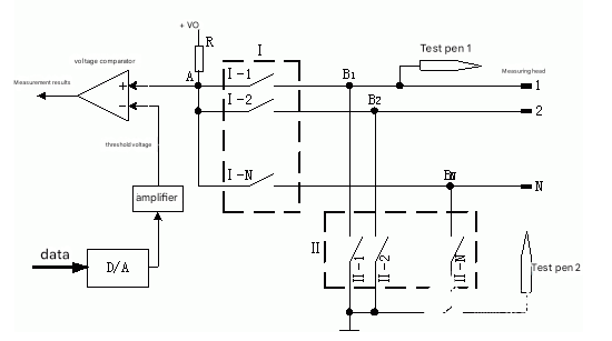
In terms of testing methods, single-layer boards and double-layer boards also use similar testing methods. Common testing methods include electrical testing and functional testing. Electrical testing is used to check the conductivity and insulation of the circuit board to ensure that there is no short circuit or open circuit. Functional testing is used to verify the performance of the circuit board under actual working conditions to ensure that it can operate normally. Whether it is a single-layer board or a double-layer board, testing is an important part of ensuring product quality.
In summary, single-layer boards and double-layer boards have many similarities in materials, manufacturing processes, application fields, design rules and testing methods. These similarities not only reflect the basic principles and technical requirements of PCB manufacturing, but also provide designers and manufacturers with unified standards and specifications, thereby ensuring the quality and reliability of electronic products.