Complete pcb manufacturing process
Overview Of The PCB Manufacturing Process
The complete process of manufacturing a printed circuit board (PCB) is a complex and intricate procedure that involves several stages, each crucial to the creation of a functional and reliable electronic component. Initially, the process begins with the design phase, where engineers utilize specialized software to create a detailed schematic of the circuit. This schematic serves as a blueprint, guiding the subsequent steps in the manufacturing process. Once the design is finalized, it is converted into a layout that specifies the exact placement of components and the routing of electrical connections.
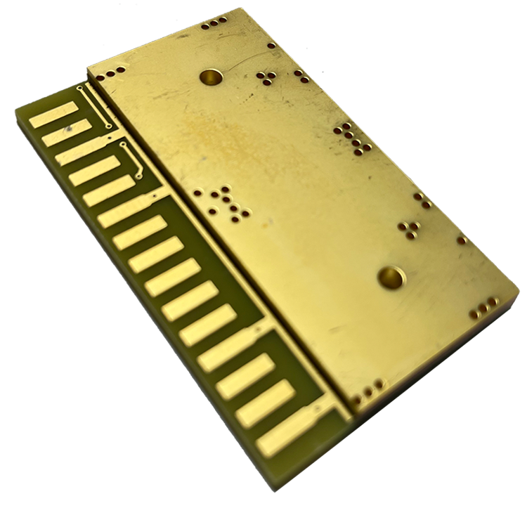
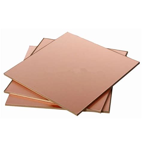
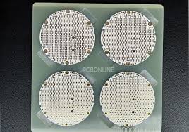
Following the design phase, the next step is the preparation of the substrate, which is typically made from a fiberglass-reinforced epoxy resin known as FR-4.
This material provides the necessary structural support and insulation for the PCB. The substrate is then coated with a thin layer of copper on both sides, which will form the conductive pathways for the electronic signals. The copper-clad substrate is then subjected to a process called photolithography, where a photosensitive film is applied to the surface. This film is exposed to ultraviolet light through a mask that represents the circuit pattern, hardening the exposed areas while leaving the unexposed areas soluble.
Subsequently, the board undergoes a chemical etching process, where the unprotected copper is removed, leaving behind the desired circuit pattern.
This step is critical, as it defines the electrical pathways that will connect the various components on the PCB. After etching, the board is thoroughly cleaned to remove any residual chemicals and debris. The next stage involves drilling holes into the board, which are necessary for mounting components and creating electrical connections between different layers of the PCB. These holes are precisely drilled using computer-controlled machines to ensure accuracy and consistency.
Once the drilling is complete, the board undergoes a plating process to deposit a thin layer of copper inside the holes, creating conductive pathways between the layers.
This is followed by the application of a solder mask, a protective layer that insulates the copper traces and prevents solder bridges during component assembly. The solder mask is typically green, although other colors are also used. The application of a silkscreen layer follows, which adds labels and markings to the board, aiding in component placement and identification.
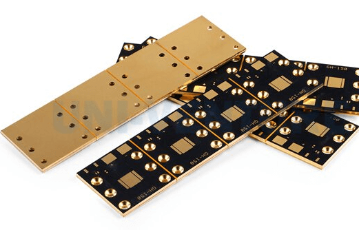
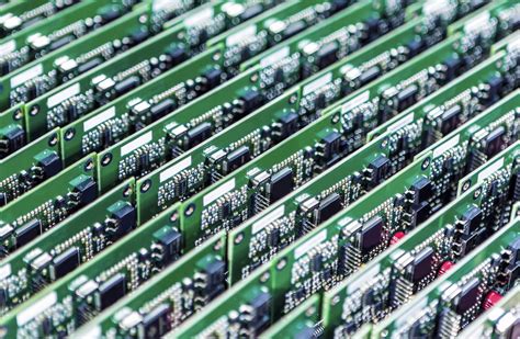
The final stages of PCB manufacturing involve the assembly of components onto the board.
This is achieved through either surface-mount technology (SMT) or through-hole technology, depending on the design requirements. SMT involves placing components directly onto the surface of the board, while through-hole technology requires inserting component leads into the drilled holes. Once the components are in place, the board is subjected to a soldering process, which secures the components and ensures electrical connectivity.
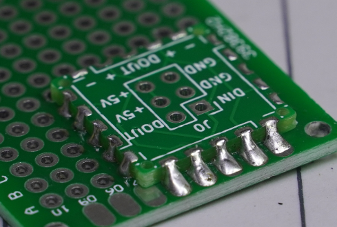
After assembly, the PCB undergoes rigorous testing to verify its functionality and reliability.
This includes electrical testing to check for short circuits and open circuits, as well as functional testing to ensure that the board performs as intended. Any defects identified during testing are addressed through rework or repair processes. Finally, the completed PCB is inspected for quality assurance before being packaged and shipped to the customer. Throughout the entire manufacturing process, strict quality control measures are implemented to ensure that the final product meets the required specifications and standards.
Key Steps In PCB Design And Layout
The process of designing and laying out a printed circuit board (PCB) is a critical phase in the development of electronic devices. It involves a series of methodical steps that ensure the final product meets the desired specifications and functions efficiently. Initially, the process begins with defining the requirements and specifications of the PCB. This involves understanding the electrical and mechanical constraints, which are crucial for the subsequent design stages. Engineers must consider factors such as the size of the board, the number of layers, and the type of components to be used. These considerations form the foundation upon which the entire design is built.
Once the requirements are clearly defined, the next step is schematic capture.
This involves creating a detailed diagram that represents the electrical connections between different components. The schematic serves as a blueprint for the PCB and is essential for ensuring that all components are correctly connected. During this phase, engineers use specialized software tools to draw the schematic, which helps in visualizing the circuit and making necessary adjustments before proceeding further.
Following the schematic capture, the process moves to the component placement stage.
This is where the physical layout of the components on the PCB is determined. Proper placement is crucial as it affects the board’s performance, manufacturability, and reliability. Engineers must strategically position components to minimize signal interference and ensure efficient heat dissipation. Additionally, they must consider the ease of assembly and testing, which can significantly impact production costs and time.
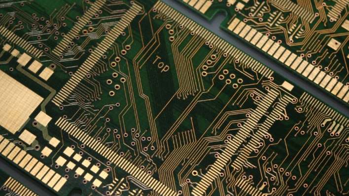
After component placement, the next step is routing, which involves connecting the components with copper traces.
This is a complex task that requires careful planning to avoid issues such as crosstalk, impedance mismatches, and signal integrity problems. Engineers use advanced routing algorithms and tools to optimize the path of the traces, ensuring that they meet the electrical and mechanical constraints defined earlier. The routing process is iterative, often requiring multiple revisions to achieve the desired performance and reliability.
Once routing is complete, the design undergoes a series of checks and validations.
This includes design rule checks (DRC) and electrical rule checks (ERC) to ensure that the layout adheres to the specified guidelines and that there are no errors in the connections. These checks are vital for identifying potential issues that could affect the functionality of the PCB. Additionally, signal integrity analysis and thermal simulations are conducted to assess the board’s performance under various conditions.
Following successful validation, the design is finalized and prepared for manufacturing.
This involves generating the necessary files, such as Gerber files, which are used by manufacturers to produce the PCB. These files contain detailed information about the board’s layout, including the copper layers, solder mask, and silkscreen. It is essential to ensure that these files are accurate and complete, as any errors can lead to costly manufacturing defects.
In conclusion, the PCB design and layout process is a meticulous and iterative endeavor that requires careful planning and execution. Each step, from defining requirements to finalizing the design, plays a crucial role in ensuring the success of the final product. By adhering to best practices and utilizing advanced tools, engineers can create PCBs that meet the desired specifications and perform reliably in their intended applications.
Advanced Techniques In PCB Fabrication
The complete PCB manufacturing process is a sophisticated sequence of steps that transforms a simple design into a functional printed circuit board, essential for modern electronic devices. As technology advances, so do the techniques employed in PCB fabrication, allowing for greater precision, efficiency, and complexity in the final product. Understanding these advanced techniques is crucial for anyone involved in the electronics industry, as they significantly impact the performance and reliability of electronic devices.
Initially, the process begins with the design phase, where engineers use specialized software to create a detailed layout of the circuit.
This digital blueprint is critical, as it dictates the placement of components and the routing of electrical connections. Once the design is finalized, it is converted into a format suitable for manufacturing, typically a Gerber file. This file serves as the foundation for the subsequent steps in the fabrication process.
Following the design phase, the next step involves the creation of the PCB substrate, which serves as the board’s backbone.
This substrate is usually made from a fiberglass-reinforced epoxy resin, known as FR-4, which provides the necessary mechanical support and electrical insulation. The substrate is then coated with a thin layer of copper on both sides, which will form the conductive pathways of the circuit.
The subsequent step is the application of a photosensitive resist to the copper-clad substrate.
This resist is exposed to ultraviolet light through a photomask, which is derived from the Gerber file. The areas exposed to light harden, while the unexposed regions remain soft and are subsequently washed away, revealing the underlying copper. This process, known as photolithography, is crucial for defining the intricate patterns of the circuit.
Once the resist is developed, the board undergoes an etching process to remove the unwanted copper, leaving behind only the desired circuit traces.
This is typically achieved using a chemical solution, such as ferric chloride or ammonium persulfate, which dissolves the excess copper. The remaining resist is then stripped away, exposing the clean copper traces that form the circuit.
To ensure the board’s durability and performance, a solder mask is applied over the entire surface, except for the areas where components will be soldered.
This protective layer prevents solder bridges and corrosion, enhancing the board’s longevity. Additionally, a silkscreen layer is often added to provide labels and markings for component placement, further aiding in assembly and troubleshooting.
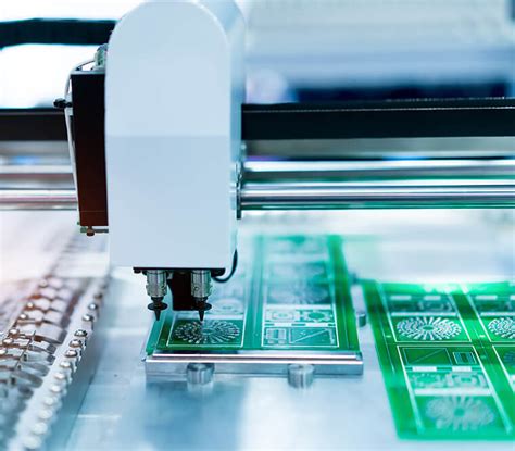
Drilling is another critical step in the PCB manufacturing process, as it creates the necessary holes for component leads and vias, which are used to connect different layers of the board. Advanced techniques, such as laser drilling, allow for precise and efficient creation of these holes, especially in high-density and multilayer boards.
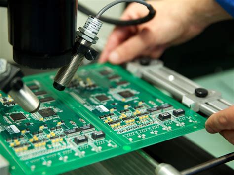
Finally, the board undergoes a series of inspections and tests to ensure its quality and functionality.
Automated optical inspection (AOI) and electrical testing are commonly employed to detect any defects or discrepancies in the circuit. Once the board passes these rigorous checks, it is ready for assembly, where components are soldered onto the board to create a complete electronic device.
In conclusion, the complete PCB manufacturing process is a complex and highly technical endeavor that requires a deep understanding of advanced fabrication techniques. As technology continues to evolve, so too will the methods used in PCB production, driving innovation and enabling the creation of increasingly sophisticated electronic devices.
Quality Control And Testing In PCB Production
In the realm of printed circuit board (PCB) manufacturing, quality control and testing are pivotal stages that ensure the reliability and functionality of the final product. As PCBs serve as the backbone of electronic devices, any defects or failures can lead to significant operational issues. Therefore, implementing rigorous quality control measures and comprehensive testing protocols is essential to uphold the integrity of the manufacturing process.
Initially, quality control begins with the inspection of raw materials.
Ensuring that the substrates, copper foils, and other components meet specified standards is crucial. This preliminary step helps in identifying any discrepancies that could potentially affect the subsequent stages of production. By employing advanced material analysis techniques, manufacturers can detect impurities or inconsistencies early on, thereby preventing defects from propagating through the manufacturing process.
As the production progresses, the focus shifts to monitoring the fabrication processes.
This includes the etching, drilling, and layering stages, where precision is paramount. Automated optical inspection (AOI) systems are commonly utilized to examine the PCBs for any deviations from the design specifications. These systems use high-resolution cameras and sophisticated algorithms to detect anomalies such as misalignments, shorts, or open circuits. By identifying these issues at an early stage, manufacturers can make necessary adjustments, thus minimizing waste and rework.
Following the fabrication, the PCBs undergo electrical testing to verify their functionality.
This is typically achieved through in-circuit testing (ICT) and flying probe testing. In-circuit testing involves using a bed of nails fixture to make contact with the test points on the PCB, allowing for the assessment of individual components and connections. On the other hand, flying probe testing employs movable probes to test the electrical performance without the need for a custom fixture. Both methods are instrumental in detecting faults such as incorrect component values, missing components, or soldering defects.
Moreover, environmental testing plays a significant role in quality assurance.
PCBs are subjected to various stress tests to evaluate their performance under different conditions. Thermal cycling tests, for instance, expose the boards to extreme temperature variations to assess their durability and reliability. Similarly, humidity and vibration tests simulate real-world conditions to ensure that the PCBs can withstand the rigors of their intended applications. These tests are crucial in identifying potential weaknesses that could lead to failures in the field.
In addition to these testing methodologies, manufacturers often implement statistical process control (SPC) to monitor and control the production process.
By analyzing data collected from various stages of manufacturing, SPC helps in identifying trends and variations that could indicate potential quality issues. This proactive approach enables manufacturers to address problems before they escalate, thereby maintaining a consistent level of quality throughout the production cycle.
Finally, documentation and traceability are integral components of the quality control process.
Detailed records of inspections, tests, and corrective actions provide a comprehensive overview of the manufacturing process. This not only facilitates continuous improvement but also ensures compliance with industry standards and regulations.
In conclusion, quality control and testing are indispensable elements of PCB production, ensuring that the final products meet the highest standards of reliability and performance. Through meticulous inspection, advanced testing techniques, and robust process control, manufacturers can deliver PCBs that are not only functional but also capable of withstanding the demands of modern electronic applications.