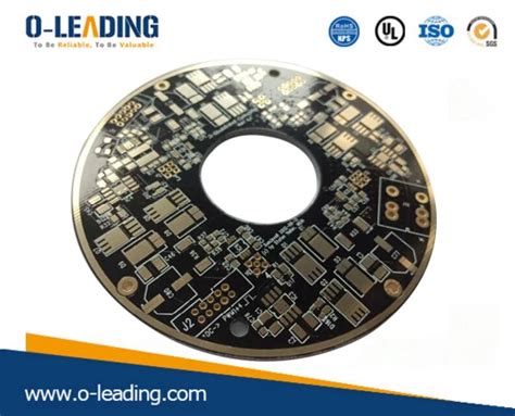
Complete pcb manufacturing process
Understanding The Basics Of PCB Design And Layout
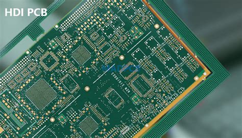
Printed Circuit Boards (PCBs) are the backbone of modern electronic devices, serving as the foundation upon which electronic components are mounted and interconnected. Understanding the basics of PCB design and layout is crucial for anyone involved in electronics manufacturing or design. The process begins with a clear understanding of the circuit’s requirements, which involves defining the electrical parameters, such as voltage, current, and signal integrity. This initial step is critical, as it sets the stage for the entire design process.
Once the requirements are established, the next phase involves schematic design.
This step translates the electrical requirements into a visual representation using specialized software. The schematic serves as a blueprint, detailing how each component is connected. It is essential to ensure accuracy at this stage, as any errors can propagate through the subsequent steps, leading to costly revisions.
Following the schematic design, the focus shifts to the layout of the PCB.
This involves arranging the physical components on the board and routing the electrical connections between them. The layout process is a delicate balance between functionality and manufacturability. Designers must consider factors such as component placement, trace routing, and layer stack-up. Proper component placement is vital for optimizing performance and minimizing electromagnetic interference. Additionally, trace routing must be carefully planned to ensure signal integrity and minimize crosstalk.
As the layout progresses, designers must also consider thermal management.
Electronic components generate heat, and without proper thermal management, this can lead to performance degradation or failure. Techniques such as adding thermal vias, using heat sinks, and optimizing trace width can help dissipate heat effectively. Moreover, the choice of materials for the PCB substrate can significantly impact thermal performance.
Once the layout is finalized, the design undergoes a series of checks to ensure compliance with design rules and manufacturing capabilities.
Design rule checks (DRC) verify that the layout adheres to predefined constraints, such as minimum trace width and spacing. Simultaneously, electrical rule checks (ERC) ensure that the design meets the electrical requirements specified in the schematic. These checks are crucial for identifying potential issues before the board is fabricated.
After passing these checks, the design is ready for fabrication.
The fabrication process involves several steps, including the creation of photomasks, etching of copper layers, and application of solder mask and silkscreen. Each step must be executed with precision to ensure the final product meets the desired specifications. The choice of fabrication techniques and materials can significantly impact the board’s performance and cost.
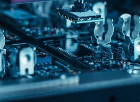
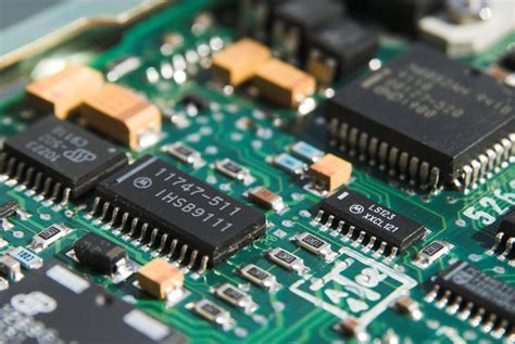
Finally, the manufactured PCB undergoes assembly, where components are soldered onto the board.
This step requires careful attention to detail, as improper soldering can lead to defects such as shorts or open circuits. Once assembled, the PCB is subjected to rigorous testing to verify its functionality and reliability.
In conclusion, understanding the basics of PCB design and layout is essential for creating reliable and efficient electronic devices. From defining electrical requirements to final assembly and testing, each step in the process requires careful consideration and expertise. By mastering these fundamentals, designers can ensure that their PCBs meet the demands of modern electronics, paving the way for innovation and advancement in the field.
Step-By-Step Guide To PCB Fabrication Techniques
The complete process of printed circuit board (PCB) manufacturing is a meticulous and intricate procedure that involves several stages, each crucial to the creation of a functional and reliable electronic component. Understanding these steps is essential for anyone involved in electronics design and production. Initially, the process begins with the design phase, where engineers use specialized software to create a detailed schematic of the circuit. This schematic is then translated into a layout that specifies the placement of components and the routing of electrical connections on the board.
Once the design is finalized, the next step is to prepare the materials.
The base of a PCB is typically made from a non-conductive substrate, such as fiberglass, which is coated with a thin layer of conductive copper. This copper layer is essential for forming the electrical pathways. The design layout is transferred onto the copper-clad board using a process called photolithography. In this process, a photosensitive film is applied to the board, and ultraviolet light is used to harden the film in areas that correspond to the circuit design. The unhardened film is then washed away, leaving a precise pattern of the circuit on the board.
Following the photolithography stage, the board undergoes an etching process.
During etching, a chemical solution removes the unwanted copper, leaving only the copper traces that form the circuit. This step is critical, as it defines the electrical pathways that will connect the various components. After etching, the board is thoroughly cleaned to remove any residual chemicals and debris.
The next phase involves drilling holes into the board.
These holes are necessary for mounting components and creating vias, which are conductive pathways that allow electrical connections between different layers of the board. Precision drilling machines are used to ensure accuracy and consistency in hole placement and size.
Subsequently, the board undergoes a plating process.
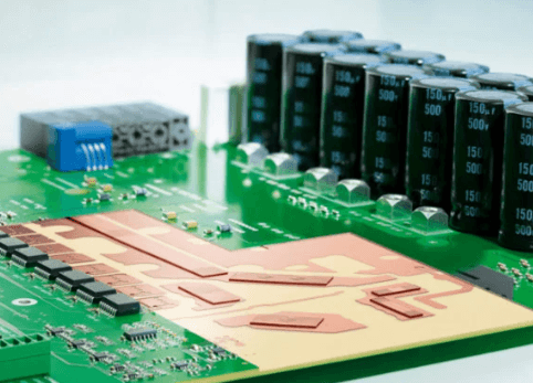
In this step, a thin layer of metal, usually tin or nickel, is deposited onto the exposed copper traces and through the drilled holes. This plating enhances the conductivity and durability of the connections. Additionally, a solder mask is applied to the board to protect the copper traces from oxidation and to prevent solder bridges during component assembly. The solder mask is typically a green epoxy resin, although other colors are also used.
Once the board is plated and masked, it is ready for the application of the silkscreen layer.
This layer contains printed information such as component labels, logos, and other identifiers that assist in the assembly and testing of the PCB. The silkscreen is applied using a screen-printing process, which ensures clarity and precision.
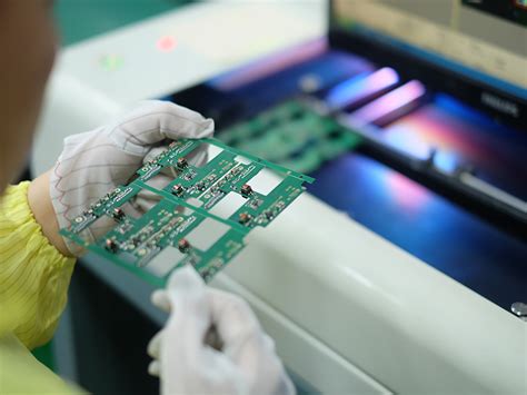
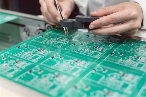
Finally, the PCB undergoes a series of inspections and tests to verify its functionality and quality.
These tests may include electrical testing to check for continuity and shorts, as well as visual inspections to ensure that the board meets design specifications. Any defects identified during testing are addressed before the board is approved for assembly.
In conclusion, the complete PCB manufacturing process is a complex sequence of steps that requires precision and attention to detail. Each stage, from design to testing, plays a vital role in ensuring the production of high-quality PCBs that meet the demands of modern electronic devices. Understanding this process is essential for anyone involved in the field of electronics manufacturing.
The Role Of Soldering In PCB Assembly
In the intricate world of printed circuit board (PCB) manufacturing, soldering plays a pivotal role in the assembly process, serving as the linchpin that ensures electrical connectivity and mechanical stability. As the demand for more compact and efficient electronic devices grows, the precision and reliability of soldering techniques have become increasingly critical. Understanding the role of soldering in PCB assembly requires a comprehensive examination of its functions, methods, and the challenges it addresses.
Soldering, at its core, involves the use of a filler metal, known as solder, to join electronic components to the PCB.
This process is essential for establishing the electrical connections that allow the components to communicate and function as intended. The solder, typically an alloy of tin and lead or other lead-free compositions, melts at a relatively low temperature, creating a bond between the component leads and the copper pads on the PCB. This bond is crucial not only for electrical conductivity but also for providing mechanical support to the components, ensuring they remain securely attached to the board.
Transitioning to the methods of soldering, there are several techniques employed in PCB assembly, each with its own advantages and applications.
The most common methods include wave soldering, reflow soldering, and hand soldering. Wave soldering is often used for through-hole components, where the PCB is passed over a wave of molten solder, allowing the solder to adhere to exposed metal surfaces. This method is efficient for mass production but may not be suitable for more delicate or densely packed boards.
Reflow soldering, on the other hand, is predominantly used for surface-mount technology (SMT) components.
In this process, solder paste is first applied to the PCB, and components are placed on top. The assembly is then heated in a reflow oven, causing the solder paste to melt and form solid connections as it cools. Reflow soldering is highly precise and can accommodate the miniaturization trends in modern electronics, making it a preferred choice for complex PCBs.
Hand soldering, while less common in large-scale manufacturing, remains invaluable for prototyping, repairs, and small-batch production.
It allows for meticulous control and is often used when automated methods are impractical. Despite its advantages, hand soldering requires skilled technicians to ensure quality and consistency.
As we delve deeper into the challenges soldering addresses, it is important to consider the issues of thermal management and reliability. Soldering must be performed at temperatures that do not damage sensitive components, necessitating careful control of the heating process. Moreover, the reliability of solder joints is paramount, as poor connections can lead to device failure. Factors such as thermal cycling, mechanical stress, and environmental conditions can all impact the longevity of solder joints, making quality control and testing essential components of the soldering process.
In conclusion, soldering is an indispensable element of PCB assembly, bridging the gap between design and functionality.
Its role extends beyond mere connectivity, encompassing the mechanical integrity and reliability of electronic devices. As technology continues to evolve, the methods and materials used in soldering will undoubtedly advance, further cementing its significance in the ever-expanding realm of electronics manufacturing. Through continuous innovation and adherence to stringent quality standards, soldering will remain a cornerstone of PCB assembly, ensuring the seamless operation of the devices that power our modern world.
Quality Control Measures In PCB Manufacturing
In the realm of printed circuit board (PCB) manufacturing, quality control measures are paramount to ensure the reliability and functionality of the final product. The intricate nature of PCBs, which serve as the backbone of electronic devices, necessitates a rigorous quality control process to detect and rectify any potential defects. This process begins with the careful selection of raw materials, as the quality of these materials directly impacts the performance and durability of the PCB. Manufacturers often source materials from reputable suppliers and conduct thorough inspections to verify their compliance with industry standards.
As the manufacturing process progresses, each stage is meticulously monitored to maintain high-quality standards.
During the initial phase of PCB fabrication, the design is transferred onto the board through a process known as photolithography. Here, precision is crucial, and any deviation can lead to significant issues in the final product. To mitigate this risk, manufacturers employ advanced imaging technologies and automated optical inspection (AOI) systems to ensure that the design is accurately replicated on the board.
Following the imaging process, the etching stage removes excess copper to reveal the circuit pattern.
This step is critical, as any over-etching or under-etching can compromise the board’s functionality. To address this, manufacturers implement stringent process controls and conduct regular inspections to verify the integrity of the etched patterns. Additionally, chemical analysis is often performed to ensure that the etching solutions are within specified parameters, further safeguarding the quality of the PCB.
Subsequently, the drilled holes, which facilitate electrical connections between different layers of the PCB, undergo a thorough inspection
Precision drilling is essential, as any misalignment can lead to connectivity issues. Manufacturers utilize high-precision drilling equipment and employ X-ray inspection techniques to verify the accuracy of the drilled holes. This step is followed by the plating process, where the holes are coated with a conductive material to establish electrical connections. The plating thickness is carefully monitored, and cross-sectional analysis is conducted to ensure uniformity and adherence to specifications.
As the PCB nears completion, solder mask application and silkscreen printing are performed.
These processes require meticulous attention to detail, as any misapplication can affect the board’s performance and readability. Automated inspection systems are employed to detect any discrepancies, ensuring that the solder mask and silkscreen are applied accurately and consistently.
Finally, the assembled PCB undergoes functional testing to verify its performance under real-world conditions.
This involves subjecting the board to various electrical tests, such as in-circuit testing (ICT) and functional testing, to ensure that it meets the required specifications. Any defects identified during this stage are analyzed, and corrective actions are implemented to prevent recurrence.
In conclusion, quality control measures in PCB manufacturing are integral to producing reliable and high-performance circuit boards. By implementing a comprehensive quality control process that encompasses every stage of production, manufacturers can ensure that their products meet the stringent demands of the electronics industry. Through continuous monitoring, advanced inspection technologies, and rigorous testing, the integrity and functionality of PCBs are preserved, ultimately contributing to the success of electronic devices in which they are utilized.
Innovations In PCB Testing And Inspection Methods
In the rapidly evolving field of electronics, the demand for high-quality printed circuit boards (PCBs) has never been greater. As the backbone of electronic devices, PCBs must meet stringent quality standards to ensure reliability and performance. Consequently, innovations in PCB testing and inspection methods have become crucial to the manufacturing process. These advancements not only enhance the accuracy and efficiency of quality control but also help manufacturers meet the increasing complexity of modern electronic designs.
To begin with, automated optical inspection (AOI) has emerged as a pivotal innovation in PCB testing.
AOI systems utilize high-resolution cameras and sophisticated algorithms to detect defects such as soldering errors, component misalignments, and surface irregularities. By comparing the captured images against a predefined set of standards, AOI systems can quickly identify discrepancies, thereby reducing the likelihood of defective boards reaching the next stage of production. Moreover, the integration of machine learning into AOI systems has further improved their ability to recognize and adapt to new defect patterns, enhancing their overall effectiveness.
In addition to AOI, X-ray inspection has gained prominence as a non-destructive testing method for PCBs.
this technique is particularly valuable for examining the integrity of solder joints and internal connections that are not visible to the naked eye. By providing a detailed view of the board’s internal structure, X-ray inspection allows manufacturers to identify hidden defects that could compromise the functionality of the final product. Furthermore, advancements in 3D X-ray imaging have enabled more comprehensive analyses, offering insights into the volumetric properties of solder joints and other critical components.
Another significant innovation in PCB testing is the development of flying probe testers.
Unlike traditional in-circuit testing methods that require custom test fixtures, flying probe testers use multiple probes that move across the board to test electrical connections. This flexibility makes them ideal for low-volume production runs and prototype testing, where the cost and time associated with creating custom fixtures are prohibitive. Additionally, flying probe testers can be easily reprogrammed to accommodate design changes, providing a versatile solution for dynamic manufacturing environments.
Moreover, the advent of functional testing has revolutionized the way PCBs are evaluated.
Unlike other methods that focus on individual components or connections, functional testing assesses the board’s performance as a whole. By simulating real-world operating conditions, functional testing ensures that the PCB will function correctly in its intended application. This holistic approach not only identifies defects that might be missed by other testing methods but also provides valuable feedback for design improvements.
As the complexity of electronic devices continues to increase, the role of advanced testing and inspection methods in PCB manufacturing becomes even more critical. Innovations such as AOI, X-ray inspection, flying probe testers, and functional testing have significantly enhanced the ability of manufacturers to produce high-quality PCBs that meet the demands of modern technology. By integrating these cutting-edge techniques into their production processes, manufacturers can ensure that their products are both reliable and efficient, ultimately contributing to the advancement of the electronics industry as a whole. As we look to the future, it is clear that continued innovation in PCB testing and inspection will be essential to keeping pace with the ever-evolving landscape of electronic design and manufacturing.