Comprehensive PCB Failure Analysis: Techniques, Causes, and Solutions
1. Introduction
Printed Circuit Boards (PCBs) are the backbone of modern electronic devices, providing mechanical support and electrical connections between components. However, PCB failures can lead to catastrophic consequences, including system malfunctions, safety hazards, and financial losses. Therefore, conducting a thorough PCB failure analysis (FA) is critical to identifying root causes, improving design, and ensuring reliability.
This article provides a comprehensive guide to PCB failure analysis, covering common failure modes, analytical techniques, and preventive measures.
2. Common PCB Failure Modes
PCB failures can occur due to manufacturing defects, material degradation, environmental stress, or design flaws. The most common failure modes include:
2.1 Electrical Failures
- Open Circuits: Broken traces due to mechanical stress, corrosion, or poor soldering.
- Short Circuits: Unintended connections caused by conductive debris, solder bridges, or dendrite growth.
- Intermittent Connections: Loose contacts or cracked solder joints leading to erratic behavior.
2.2 Mechanical Failures
- Delamination: Separation of PCB layers due to moisture absorption or thermal stress.
- Cracks in Substrate: Mechanical stress or thermal cycling causing fractures in the PCB material.
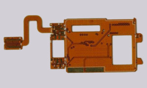
- Flexural Failures: Bending or twisting leading to trace fractures in flexible PCBs.
2.3 Thermal Failures
- Thermal Fatigue: Repeated heating/cooling cycles weakening solder joints.
- Overheating: Excessive current or poor thermal management causing burnt traces or component failure.
2.4 Environmental Failures
- Corrosion: Oxidation of copper traces due to humidity or chemical exposure.
- Conductive Anodic Filament (CAF) Growth: Ionic contamination leading to electrical leakage between traces.
2.5 Manufacturing Defects
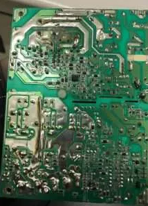
- Poor Soldering: Cold solder joints, voids, or insufficient wetting.
- Misaligned Drills: Incorrectly drilled holes affecting component placement.
- Contamination: Flux residues or metallic particles causing short circuits.
3. PCB Failure Analysis Techniques
To diagnose PCB failures, engineers use a combination of non-destructive and destructive testing methods.
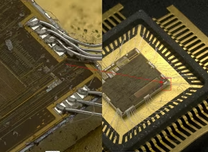
3.1 Visual Inspection (VI)
- Optical Microscopy: Identifies solder defects, cracks, and contamination.
- X-ray Inspection: Reveals hidden defects like voids in solder joints or internal delamination.
3.2 Electrical Testing
- Continuity Testing: Checks for open/short circuits.
- In-Circuit Testing (ICT): Validates component functionality.
- Time-Domain Reflectometry (TDR): Locates impedance mismatches in high-speed PCBs.
3.3 Thermal Analysis
- Infrared (IR) Thermography: Detects hotspots and thermal anomalies.
- Thermal Cycling Tests: Simulates real-world temperature variations.
3.4 Material Analysis
- Scanning Electron Microscopy (SEM): Examines microstructure and fracture surfaces.
- Energy-Dispersive X-ray Spectroscopy (EDS): Identifies elemental composition of contaminants.
- Fourier Transform Infrared Spectroscopy (FTIR): Detects organic residues.
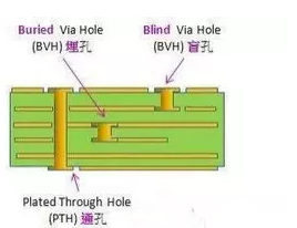
3.5 Cross-Sectional Analysis
- Microsectioning: Cuts PCB samples to inspect internal layer defects.
- Acid Decapsulation: Removes encapsulation to examine wire bonds and die attach.
3.6 Environmental Stress Testing
- Humidity Testing (HAST/T/H): Evaluates moisture resistance.
- Vibration & Shock Testing: Assesses mechanical robustness.
4. Root Cause Analysis (RCA) and Corrective Actions
Once failure modes are identified, Root Cause Analysis (RCA) helps determine underlying issues and implement corrective actions.
4.1 Design-Related Failures
- Solution: Optimize trace width, spacing, and thermal reliefs. Use simulation tools (e.g., Ansys, Cadence) to predict failures.
4.2 Manufacturing Defects
- Solution: Improve soldering processes (reflow profile optimization), enforce cleanliness standards, and implement Automated Optical Inspection (AOI).
4.3 Material Degradation
- Solution: Select high-Tg (glass transition temperature) materials for high-temperature applications. Use conformal coatings for moisture protection.
4.4 Environmental Stress
- Solution: Apply protective coatings, use hermetic sealing, and design for thermal dissipation.
5. Case Studies in PCB Failure Analysis
Case 1: Solder Joint Fatigue in Automotive Electronics
- Failure Mode: Intermittent failures in engine control modules.
- Analysis: Cross-sectioning revealed cracked solder joints due to thermal cycling.
- Solution: Use of SAC305 (lead-free) solder with improved fatigue resistance.
Case 2: CAF Growth in High-Humidity Environments
- Failure Mode: Short circuits between plated through-holes.
- Analysis: SEM/EDS detected copper dendrites due to ionic contamination.
- Solution: Improved PCB cleaning and low-halogen laminate materials.
6. Preventive Measures & Best Practices
To minimize PCB failures, follow these best practices:
✔ Design for Reliability (DFR): Follow IPC standards (e.g., IPC-7351 for land patterns).
✔ Robust Manufacturing Controls: Implement SPI (Solder Paste Inspection) and AOI.
✔ Environmental Protection: Use conformal coatings for harsh environments.
✔ Regular Testing: Perform accelerated life testing (ALT) and HALT (Highly Accelerated Life Testing).
7. Conclusion
PCB failure analysis is a multidisciplinary process involving electrical, mechanical, thermal, and material science expertise. By leveraging advanced analytical techniques and implementing corrective actions, manufacturers can enhance PCB reliability and prevent costly failures.
Investing in proactive failure analysis not only improves product quality but also extends the lifespan of electronic systems in industries ranging from consumer electronics to aerospace and medical devices.