Consumer Electronics PCB: Design, Manufacturing, and Industry Trends
Introduction
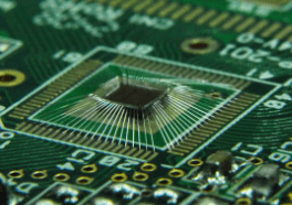
Printed Circuit Boards (PCBs) are the backbone of modern consumer electronics, enabling the functionality of devices we use daily, such as smartphones, laptops, wearables, and smart home systems. As consumer demand for compact, high-performance, and energy-efficient devices grows, PCB technology continues to evolve to meet these challenges.
This article explores the role of PCBs in consumer electronics, key design considerations, manufacturing processes, and emerging trends shaping the industry.
1. The Role of PCBs in Consumer Electronics
PCBs serve as the foundation for electronic circuits, providing mechanical support and electrical connections between components. In consumer electronics, PCBs must meet stringent requirements, including:
- Miniaturization – Devices like smartphones and wearables demand compact PCB designs with high-density interconnects (HDI).
- High-Speed Performance – With 5G, IoT, and AI-driven devices, PCBs must support faster signal transmission with minimal interference.
- Power Efficiency – Energy-efficient designs extend battery life in portable electronics.
- Durability – PCBs in consumer devices must withstand mechanical stress, heat, and environmental factors.
Common consumer electronics that rely on advanced PCBs include:
- Smartphones & Tablets
- Laptops & Wearables
- Smart TVs & Home Appliances
- Gaming Consoles & VR Devices
- Wireless Earbuds & Smart Speakers
2. Key PCB Design Considerations for Consumer Electronics
2.1. High-Density Interconnect (HDI) PCBs
As devices shrink, HDI PCBs use microvias, thinner traces, and stacked layers to maximize space efficiency. This is crucial for smartphones and wearables where space is limited.
2.2. Flexible and Rigid-Flex PCBs
- Flexible PCBs (FPCs) – Used in foldable phones, wearables, and curved displays.
- Rigid-Flex PCBs – Combine rigid and flexible sections, ideal for compact, durable designs like cameras and medical wearables.
2.3. Thermal Management
Consumer electronics generate heat, especially in high-performance devices like gaming laptops. Designers use:
- Thermal vias
- Heat sinks
- High-thermal-conductivity materials
2.4. Signal Integrity & EMI Shielding
High-speed data transmission (e.g., 5G, Wi-Fi 6) requires:
- Controlled impedance routing
- Proper grounding techniques
- EMI shielding to reduce interference
2.5. Material Selection
- FR-4 – Standard for cost-effective PCBs.
- High-Frequency Laminates (Rogers, Teflon) – For RF and 5G applications.
- Metal-Core PCBs – For LED lighting and power electronics.
3. PCB Manufacturing Process for Consumer Electronics
3.1. Design & Prototyping
- Schematic Design – Circuit layout planning using CAD tools (Altium, Eagle).
- DFM (Design for Manufacturing) Checks – Ensuring manufacturability and cost efficiency.
- Prototyping & Testing – Verifying performance before mass production.
3.2. PCB Fabrication
- Substrate Preparation – Cutting and cleaning the base material.
- Layer Stackup & Lamination – Building multilayer PCBs.
- Drilling & Plating – Creating vias for interlayer connections.
- Etching – Removing excess copper to form traces.
- Solder Mask & Silkscreen – Adding protective and labeling layers.
3.3. Assembly (PCBA)
- Surface Mount Technology (SMT) – Automated component placement for high-volume production.
- Through-Hole Assembly – For larger components needing stronger connections.
- Testing & Quality Control – AOI (Automated Optical Inspection), X-ray, and functional testing.

4. Emerging Trends in Consumer Electronics PCBs
4.1. Miniaturization & Wearable Tech
- Ultra-thin PCBs for foldable phones and smartwatches.
- Stretchable PCBs for next-gen wearables.
4.2. 5G & High-Speed PCBs
- Low-loss materials for millimeter-wave (mmWave) frequencies.
- Advanced signal integrity techniques for faster data transfer.
4.3. IoT & Smart Home Devices
- Low-power PCBs for battery-operated sensors.
- Embedded antennas for wireless connectivity.
4.4. Sustainable PCB Manufacturing
- Lead-free soldering and halogen-free materials.
- Recycling programs for e-waste reduction.
4.5. AI-Optimized PCB Design
- Machine learning for automated routing and defect detection.
- AI-driven thermal and signal integrity simulations.
5. Challenges in Consumer Electronics PCB Production
- Cost vs. Performance Trade-offs – Balancing advanced features with affordability.
- Supply Chain Disruptions – Semiconductor shortages affecting PCB assembly.
- Environmental Regulations – Compliance with RoHS, REACH, and WEEE standards.
- Counterfeit Components – Ensuring authentic, high-quality parts.
6. Conclusion
PCBs are at the heart of consumer electronics, driving innovation in miniaturization, connectivity, and performance. As technology advances, PCB manufacturers must adapt to trends like 5G, IoT, and AI while overcoming challenges in cost, sustainability, and supply chain stability.
By leveraging advanced materials, smart manufacturing, and cutting-edge design techniques, the PCB industry will continue to power the next generation of consumer devices.


