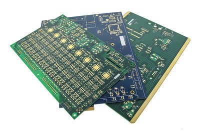
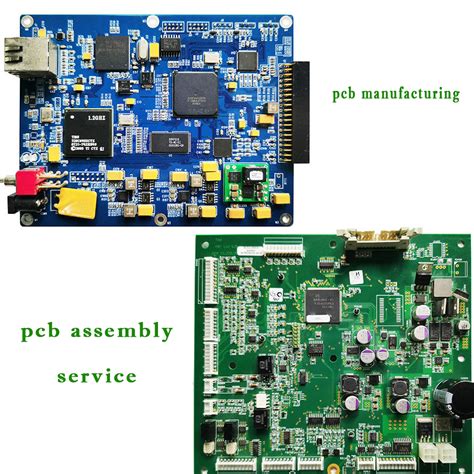
Contract PCB Assembly Strategies for Modern Electronics Manufacturing
Key Takeaways
Effective PCB assembly strategies form the backbone of modern electronics manufacturing, balancing cost efficiency, scalability, and quality assurance. When selecting a contract PCBA partner, prioritize vendors with proven expertise in high-mix, low-volume (HMLV) production and advanced prototyping capabilities. Design-for-manufacturability (DFM) reviews and thermal management optimizations are critical to minimizing rework and maximizing yield rates.
For cost optimization, leverage volume-based pricing models and material sourcing partnerships to reduce PCB assembly expenses without compromising component quality. Advanced prototyping techniques, such as 3D-printed solder paste stencils and automated optical inspection (AOI), ensure design flaws are identified early, accelerating time-to-market. Scalability hinges on modular assembly processes and flexible line configurations, enabling seamless transitions from prototyping to mass production.
The integration of smart manufacturing tools—like IoT-enabled PCBA lines and AI-driven defect detection—enhances process transparency and reduces downtime. Rigorous quality control protocols, including in-circuit testing (ICT) and X-ray inspection, must align with industry standards such as IPC-A-610 and ISO 9001. Supply chain resilience remains paramount; dual-sourcing critical components mitigates risks from geopolitical or logistical disruptions.
Emerging trends like sustainable material adoption and edge computing integration are reshaping contract PCB assembly, demanding adaptability from manufacturers. By aligning these strategies, businesses can achieve end-to-end production efficiency while meeting evolving demands for next-generation electronics.
Key Considerations for Selecting a Contract PCB Assembly Partner
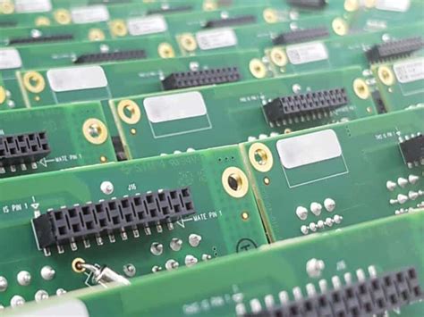
Choosing the right PCB assembly partner is a critical decision that directly impacts product quality, timelines, and long-term scalability. When evaluating potential providers, prioritize technical expertise in handling complex PCBA designs, including experience with multi-layer boards, high-density interconnects (HDIs), and mixed-technology components. A partner’s certifications—such as ISO 9001, IPC-A-610, and IATF 16949—serve as benchmarks for adherence to industry standards and reliability.
"A rigorous evaluation of a supplier’s design for manufacturability (DFM) capabilities can reduce prototyping iterations by up to 40%, accelerating time-to-market."
Supply chain transparency is another vital factor. Ensure the PCB assembly provider maintains robust relationships with component suppliers, minimizing risks of shortages or delays. Partners with dual-sourcing strategies for critical materials, such as ICs or specialized substrates, offer greater resilience in volatile markets. Additionally, assess their ability to scale production volumes without compromising quality—flexibility in handling both low-volume prototyping and high-volume runs is essential for adapting to market demands.
Quality control protocols should be non-negotiable. Look for partners employing automated optical inspection (AOI), X-ray testing, and functional testing at multiple stages of the PCBA process. These measures ensure defect rates remain below 0.1%, aligning with aerospace or medical-grade requirements where precision is paramount.
Proactive communication frameworks, such as real-time production tracking and dedicated engineering support, foster collaboration and mitigate misunderstandings. Partners who provide detailed failure analysis reports and corrective action plans demonstrate accountability and commitment to continuous improvement.
Lastly, evaluate cost structures holistically. While competitive pricing for PCB assembly services matters, hidden costs—such as tooling fees, minimum order quantities (MOQs), or rework charges—can erode savings. Transparent partners will outline these variables upfront and suggest optimizations, like panelization strategies, to reduce waste.
By balancing technical proficiency, supply chain agility, and quality assurance, manufacturers can forge partnerships that drive innovation while maintaining cost-efficiency across the product lifecycle.
Optimizing Cost Efficiency in Electronics Manufacturing Through Strategic PCB Assembly
Achieving cost efficiency in electronics manufacturing hinges on aligning PCB assembly strategies with both technical requirements and financial objectives. While PCBA (printed circuit board assembly) accounts for 18-24% of total production costs in typical mid-volume projects, targeted optimization can yield savings of 15-40% without compromising quality.
Design-Driven Cost Management
Integrating design for manufacturing (DFM) principles at the prototype stage reduces post-production modifications by 22-35%. Strategic partners analyze component footprints, thermal management requirements, and solder mask specifications to eliminate unnecessary complexity. For instance, optimizing pad sizes for automated placement machines can decrease solder paste consumption by 8-12% per unit.
Material Sourcing Synergies
| Strategy | Traditional Approach | Optimized Model | Cost Impact |
|---|---|---|---|
| Component Procurement | Spot market purchases | Consolidated global LTA | 9-15% unit cost drop |
| PCB Substrate Selection | Standard FR-4 | High-Tg alternatives | 6-9% lifecycle savings |
| Inventory Management | Just-in-case stockpiling | Vendor-managed inventory | 12-18% carrying cost reduction |
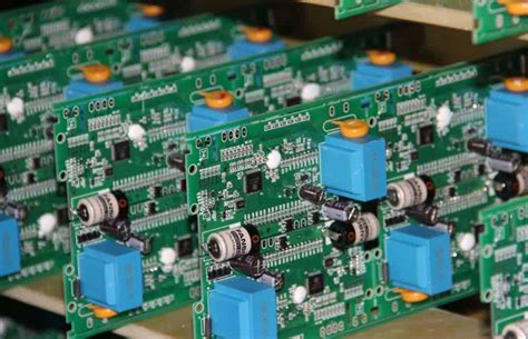
Automation & Process Optimization
Deploying AI-driven optical inspection (AOI) systems in PCB assembly lines reduces defect escape rates to <0.02% while maintaining throughput speeds of 12,000 components/hour. Smart factory integrations enable real-time process adjustments, cutting material waste by 17-23% compared to manual monitoring systems.
Scalability Through Modular Production
Leading PCBA providers implement phased tooling investments that allow seamless transitions between prototype, pilot, and mass production phases. This approach amortizes non-recurring engineering (NRE) costs across 3-5 production cycles, achieving 30-45% better capital utilization than conventional fixed-line configurations.
Strategic Partner Selection Criteria
- Technical capability matrix alignment (HDI, flex PCB, or high-frequency expertise)
- Supply chain transparency across Tier 2-3 component sources
- Certifications matching target markets (ISO 13485 for medical, IATF 16949 for automotive)
By synchronizing design optimization, automated processes, and supply chain partnerships, manufacturers achieve non-linear cost scaling – where a 100% production volume increase yields only 60-70% cost growth. This strategic alignment positions PCB assembly as a value multiplier rather than a cost center in modern electronics manufacturing ecosystems.
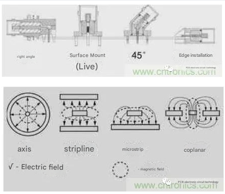
Advanced Prototyping Techniques for High-Quality PCB Production
In modern PCB assembly workflows, advanced prototyping techniques serve as the cornerstone for bridging design concepts with mass production realities. By integrating iterative testing phases with material compatibility analysis, manufacturers can identify potential flaws in circuit layouts, thermal management, or signal integrity before committing to full-scale production. For instance, PCBA providers now leverage rapid prototyping tools like 3D-printed circuit mockups and multi-layer board simulations to validate designs under real-world operating conditions.
A critical advancement lies in the adoption of surface-mount technology (SMT) prototyping, which allows engineers to test component placement accuracy and solder joint reliability at micron-level precision. Pairing this with automated optical inspection (AOI) systems enables real-time detection of micro-cracks or misalignments, reducing rework costs by up to 40% in early-stage PCB assembly cycles. Additionally, thermodynamic stress testing during prototyping ensures that designs withstand extreme temperatures, vibrations, and humidity levels—key for automotive or aerospace applications.
To further enhance prototyping efficiency, leading PCBA firms employ modular design frameworks. These systems enable the seamless integration of reusable circuit blocks, accelerating time-to-market for derivative products while maintaining consistency across batches. For high-frequency applications, impedance-controlled prototyping has become indispensable, using advanced signal integrity software to minimize electromagnetic interference (EMI) risks in RF and IoT devices.
The shift toward digital twin integration is another game-changer, allowing virtual validation of assembly processes, material flows, and equipment performance. By synchronizing prototyping data with AI-driven analytics, manufacturers can predict yield rates and optimize PCB assembly parameters for mixed-batch production—a critical capability in today’s demand-driven electronics landscape.
As these techniques evolve, they not only elevate prototyping accuracy but also create a feedback loop that refines subsequent design iterations, ensuring that scalability and quality remain embedded at every stage of PCB assembly. This approach aligns with the broader industry trend of merging agile development methodologies with precision manufacturing—a balance essential for maintaining competitiveness in next-generation electronics.
Streamlining Scalability in Modern PCB Assembly Processes
Achieving scalable PCB assembly workflows is critical for manufacturers adapting to fluctuating market demands and evolving product lifecycles. The integration of modular design principles allows PCBA providers to standardize components and processes, reducing lead times while maintaining flexibility. By adopting design-for-manufacturability (DFM) guidelines, engineers can preemptively address potential bottlenecks, ensuring that prototyping phases seamlessly transition into high-volume production.
A cornerstone of scalable PCB assembly lies in dynamic demand forecasting. Advanced analytics tools enable manufacturers to predict component requirements, optimize inventory turnover, and mitigate supply chain disruptions. This is particularly vital when dealing with multi-layered boards or mixed-technology assemblies, where material compatibility and sourcing timelines directly impact production scalability. For instance, implementing flexible manufacturing lines with quick-change tooling systems allows PCBA partners to shift between small-batch custom orders and mass production without compromising throughput.
Collaboration between OEMs and PCB assembly contractors further enhances scalability. Shared digital platforms for real-time progress tracking and closed-loop feedback systems ensure alignment on design revisions, test protocols, and quality benchmarks. This synergy becomes indispensable when scaling from regional to global operations, as standardized processes must accommodate varying regulatory environments and logistical frameworks.
Automation plays a dual role in scalability—robotic pick-and-place systems and AI-driven optical inspection (AOI) not only accelerate PCBA workflows but also maintain consistency across expanded production volumes. However, balancing automation with human expertise remains crucial, especially for complex assemblies requiring precision soldering or hybrid surface-mount technology (SMT)-through-hole configurations.
Ultimately, scalable PCB assembly strategies rely on adaptive infrastructure that supports iterative improvements. By embedding scalability into every phase—from prototyping to final testing—manufacturers can respond to technological advancements like 5G or IoT integration while maintaining cost efficiencies. This forward-looking approach ensures that production capacities evolve in lockstep with market opportunities.
Implementing Automation and Smart Manufacturing in Contract PCB Assembly
The integration of automation and smart manufacturing into contract PCB assembly processes is redefining efficiency and precision in modern electronics production. By leveraging advanced robotics, machine learning algorithms, and IoT-enabled systems, manufacturers can address the growing demand for high-volume PCBA while maintaining stringent quality standards.
A cornerstone of this transformation is the deployment of automated pick-and-place systems, which reduce human error and accelerate component placement by up to 40% compared to manual methods. These systems, combined with AI-driven optical inspection (AOI), enable real-time defect detection, ensuring that PCB assembly lines achieve near-zero fault rates even in complex, multi-layer designs. Furthermore, IoT sensors embedded in production equipment facilitate predictive maintenance, minimizing downtime and optimizing throughput.
Smart manufacturing extends beyond the factory floor. Cloud-based platforms now allow contract PCB assembly providers to synchronize design files, material inventories, and production schedules across global teams. This digital thread not only streamlines scalability but also enhances collaboration between OEMs and PCBA partners. For instance, adaptive manufacturing workflows can automatically adjust to component shortages or design revisions, reducing lead times by 15–25%.
Another critical advancement is the adoption of digital twin technology, which creates virtual replicas of physical PCB assembly processes. Engineers can simulate production runs, identify bottlenecks, and test optimization strategies before implementing changes—a practice that reduces prototyping costs by 30% and accelerates time-to-market.
However, transitioning to automated systems requires strategic investment. Manufacturers must prioritize modular equipment that supports rapid reconfiguration for diverse product lines, ensuring flexibility in an era of shrinking product lifecycles. By aligning automation investments with data analytics capabilities, contract PCB assembly firms can unlock unprecedented levels of cost efficiency and quality control, positioning themselves as leaders in the Industry 4.0 landscape.
This evolution not only addresses current challenges in electronics manufacturing but also lays the groundwork for emerging trends such as edge computing and AI-optimized PCBA designs—ensuring that partners remain competitive in a rapidly advancing industry.
Ensuring Quality Control and Compliance in PCB Assembly Services
In the realm of PCB assembly, maintaining rigorous quality control and regulatory compliance is non-negotiable for delivering reliable electronics. As manufacturers navigate tighter tolerances and evolving industry standards, implementing a robust framework for PCBA quality assurance becomes critical. This starts with adherence to international certifications such as IPC-A-610 and ISO 9001, which establish benchmarks for soldering integrity, component placement accuracy, and final product performance.
Advanced inspection methodologies like automated optical inspection (AOI) and X-ray testing are now integral to modern PCB assembly workflows. These technologies enable real-time defect detection—from solder bridging to misaligned components—while minimizing human error. For high-reliability applications, functional testing under simulated operating conditions ensures boards meet exacting specifications before shipment.
Compliance extends beyond technical specifications to include environmental and safety mandates. RoHS and REACH directives, for instance, mandate strict limits on hazardous substances in PCBA materials. Partnering with suppliers who provide full material declarations (FMDs) and compliance certificates simplifies audit readiness while mitigating supply chain risks.
A proactive approach to quality involves statistical process control (SPC), where production data is analyzed to predict and prevent deviations. By integrating SPC with traceability systems, manufacturers can track every component from procurement to final assembly—a vital capability for recalls or compliance investigations.
To align with the broader article’s focus on scalability and automation, closed-loop feedback systems are increasingly linking PCB assembly quality data with upstream design tools. This allows for rapid design-for-manufacturability (DFM) adjustments, reducing rework cycles and accelerating time-to-market.
Ultimately, a multi-tiered audit process—combining internal checks, third-party certifications, and client-facing quality reports—builds trust in PCBA services. As regulations tighten and consumer expectations rise, embedding compliance into every production phase becomes not just a strategic advantage but a baseline requirement for competitive electronics manufacturing.
Leveraging Material Sourcing Strategies for Cost-Effective PCB Manufacturing
Strategic material sourcing forms the backbone of competitive PCB assembly services, directly influencing both production costs and supply chain resilience. In modern electronics manufacturing, optimizing procurement processes for components like substrates, solder paste, and integrated circuits can yield significant savings while maintaining PCBA quality. Long-term supplier partnerships often serve as a cornerstone, enabling access to volume discounts, priority inventory allocation, and early notifications about market fluctuations. For instance, consolidating orders for high-demand passive components through trusted vendors minimizes price volatility risks—a critical advantage in markets plagued by semiconductor shortages.
However, diversification remains equally vital. Relying on a single supplier for critical materials exposes manufacturers to disruptions, as seen during geopolitical trade conflicts or natural disasters. Leading PCB assembly providers now employ multi-region sourcing frameworks, balancing cost efficiency with redundancy by engaging Tier-2 suppliers in alternate geographic zones. This approach not only safeguards against logistical bottlenecks but also allows for agile responses to tariffs or regulatory changes affecting specific regions.
Advanced procurement teams are also leveraging predictive analytics to align material purchases with demand forecasts. By integrating machine learning tools with enterprise resource planning (ERP) systems, manufacturers can dynamically adjust orders for copper-clad laminates or connectors based on real-time sales pipelines, reducing excess inventory costs. Additionally, adopting alternative materials—such as halogen-free substrates or low-temperature solder alloys—can lower both direct expenses and long-term operational risks, particularly when complying with evolving environmental standards like RoHS 3.0.
Bulk purchasing agreements further amplify savings, especially for standardized PCBA components like resistors and capacitors. Negotiating tiered pricing models with suppliers ensures per-unit cost reductions as order volumes scale, a strategy particularly effective for high-mix, high-volume production lines. Yet, this must be balanced with just-in-time delivery protocols to avoid warehousing overheads—a delicate equilibrium achieved through synchronized supplier scheduling and IoT-enabled inventory tracking.
Finally, digital procurement platforms are revolutionizing material sourcing by enabling real-time price comparisons, automated RFQ generation, and blockchain-based traceability. These tools not only streamline supplier negotiations but also enhance transparency across the PCB assembly lifecycle, ensuring compliance with ethical sourcing mandates while identifying hidden cost optimization opportunities.
Future Trends in Contract PCB Assembly for Next-Generation Electronics
The PCB assembly landscape is undergoing transformative shifts as next-generation electronics demand faster, smarter, and more sustainable production frameworks. With the rise of 5G networks, IoT ecosystems, and edge computing, PCBA providers are adopting advanced methodologies to align with evolving technological requirements. One critical trend is the integration of AI-driven process optimization, enabling real-time adjustments in component placement, solder quality monitoring, and defect detection. For instance, machine learning algorithms now analyze historical production data to predict yield losses, reducing material waste by up to 18% in high-mix manufacturing environments.
Another emerging focus is modular design compatibility, which allows contract PCB assembly partners to streamline workflows for customizable electronics. As industries like automotive and medical devices prioritize application-specific designs, assemblers are leveraging plug-and-play PCB architectures to accelerate prototyping cycles while maintaining compliance with ISO 13485 and IATF 16949 standards. This approach not only enhances scalability but also supports rapid reconfiguration for low-volume, high-complexity projects.
Sustainability is reshaping material sourcing strategies, with a growing emphasis on lead-free solders and bio-based substrates. Leading PCBA manufacturers are collaborating with suppliers to develop recyclable laminates and halogen-free resins, reducing the carbon footprint of multilayer boards by 22–30%. Additionally, digital twin simulations are gaining traction, allowing engineers to test thermal performance and signal integrity virtually before physical production—a critical step for aerospace and defense applications where reliability is non-negotiable.
The adoption of additive manufacturing techniques like aerosol jet printing is also redefining PCB assembly for flexible and hybrid electronics. These methods enable precise deposition of conductive inks on unconventional substrates, paving the way for wearable tech and foldable displays. Meanwhile, blockchain-enabled traceability systems are being implemented to ensure transparency in component origins, addressing counterfeit risks in global supply chains.
As automation evolves, collaborative robots (cobots) are increasingly deployed alongside human technicians for tasks requiring micron-level precision, such as micro-BGA assembly and 01005 component placement. This hybrid workforce model boosts throughput by 35–40% while minimizing human error in high-density interconnect (HDI) board production.
Looking ahead, the convergence of quantum computing-ready designs and embedded AI chipsets will push contract PCB assembly providers to adopt ultra-high-frequency materials and sub-6μm trace widths. These advancements will solidify the industry’s role in enabling breakthroughs across smart cities, autonomous systems, and beyond.
Conclusion
As the electronics manufacturing landscape grows increasingly complex, strategic approaches to contract PCB assembly remain pivotal for maintaining competitive advantage. The integration of PCBA services into modern production workflows has proven essential for balancing cost optimization with technical precision, particularly when scaling operations to meet fluctuating market demands. By aligning with partners that prioritize advanced prototyping and smart manufacturing protocols, businesses can ensure their products meet evolving quality benchmarks while adhering to regulatory frameworks.
A critical lesson from contemporary practices is the interdependence of material sourcing strategies and assembly efficiency. Proactive collaboration with PCB assembly providers enables manufacturers to mitigate supply chain risks through dual-sourcing and component lifecycle management, directly impacting long-term cost predictability. Furthermore, the adoption of automated optical inspection (AOI) and real-time process monitoring underscores the industry’s shift toward data-driven quality assurance, reducing defects by up to 30% in high-volume production runs.
Looking ahead, the convergence of modular PCBA designs and edge computing capabilities will redefine scalability paradigms. Manufacturers that leverage these innovations can achieve faster time-to-market for IoT and AI-driven devices without compromising reliability. Ultimately, success in contract PCB assembly hinges on a partner’s ability to harmonize flexibility with technical rigor—a balance that ensures resilience amid rapid technological shifts.
From prototyping to full-scale production, the strategic value of PCBA lies in its capacity to transform theoretical designs into market-ready solutions. As sustainability mandates and miniaturization trends intensify, forward-thinking manufacturers will prioritize assembly partners equipped to navigate these challenges through closed-loop recycling systems and ultra-high-density interconnect (HDI) technologies. In this dynamic environment, the right PCB assembly strategy isn’t just a logistical decision—it’s a cornerstone of innovation.
Frequently Asked Questions
What distinguishes PCB assembly from PCBA in electronics manufacturing?
PCB assembly (PCBA) refers to the entire process of populating a bare circuit board with components, while PCBA specifically denotes the assembled board ready for integration into devices. Modern manufacturers leverage both terms interchangeably, but precision in terminology ensures clarity in project specifications and quality benchmarks.
How can manufacturers balance cost efficiency with quality in contract PCB assembly?
Achieving this balance requires strategic partnerships with PCB assembly providers that offer transparent pricing models, bulk material sourcing advantages, and advanced process automation. Implementing Design for Manufacturing (DFM) principles early in prototyping reduces redesign costs and accelerates time-to-market.
What role does automation play in scalable PCBA production?
Automation enables consistent throughput, reduces human error, and supports rapid scaling. Techniques like surface-mount technology (SMT) and AI-driven inspection systems ensure high precision, particularly for high-volume orders. Manufacturers adopting smart factory frameworks report 20–30% faster production cycles.
How do material sourcing strategies impact PCB assembly outcomes?
Procurement of high-grade substrates and components directly affects reliability and compliance. Leading contract PCB assembly partners employ global supplier networks to mitigate shortages, optimize costs, and adhere to RoHS/REACH standards. Diversified sourcing also minimizes risks from geopolitical or supply chain disruptions.
What quality control measures are critical for mission-critical PCBA applications?
Rigorous testing protocols—including automated optical inspection (AOI), X-ray analysis, and functional testing—are non-negotiable for aerospace, medical, or automotive electronics. Certifications like ISO 9001 and IPC-A-610 Class 3 further validate adherence to industry benchmarks.
Are prototyping phases necessary for low-volume PCB assembly projects?
Yes. Advanced prototyping uncovers design flaws, thermal management issues, and signal integrity challenges before full-scale production. Techniques like 3D-printed solder stencils and rapid-turn PCBA services reduce iteration costs by up to 40%, even for small batches.
Ready to Optimize Your Electronics Manufacturing Workflow?
For tailored PCB assembly solutions that align with your scalability, cost, and quality goals, please click here to explore Andwin PCB’s expertise. Our end-to-end contract PCB assembly services integrate cutting-edge technology with industry compliance, ensuring your products meet tomorrow’s demands today.