Copper Base PCBs: A Comprehensive Guide to Design, Benefits, and Applications
Introduction
In the world of electronics, thermal management is a critical factor that directly impacts the performance, reliability, and lifespan of electronic devices. As electronic components become more powerful and compact, the need for efficient heat dissipation has grown significantly. Copper Base PCBs, also known as metal core PCBs (MCPCBs), have emerged as a leading solution for managing heat in high-power applications. These PCBs feature a copper base layer that provides exceptional thermal conductivity, making them ideal for applications such as LED lighting, power electronics, and automotive systems. This article provides a comprehensive overview of Copper Base PCBs, including their structure, design considerations, advantages, and applications.
What is a Copper Base PCB?
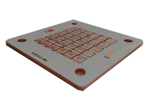
A Copper Base PCB is a type of metal core PCB that uses a thick copper layer as its base material. Unlike traditional FR-4 PCBs, which use a fiberglass substrate, Copper Base PCBs are designed to efficiently transfer heat away from high-power components. The typical structure of a Copper Base PCB consists of the following layers:
- Circuit Layer: The top layer, made of copper, where the electronic components are mounted and interconnected.
- Dielectric Layer: An insulating layer that separates the circuit layer from the copper base. This layer is designed to provide electrical insulation while maintaining high thermal conductivity.
- Copper Base Layer: A thick layer of copper that acts as a heat sink, dissipating heat generated by the components.
The copper base layer is the defining feature of these PCBs, offering superior thermal performance compared to other metal core materials such as aluminum.

Design Considerations for Copper Base PCBs
Designing a Copper Base PCB requires careful attention to thermal, electrical, and mechanical factors. Below are some key considerations:
- Thermal Management
The primary purpose of a Copper Base PCB is to dissipate heat efficiently. Designers must ensure that the copper base layer is adequately sized and connected to heat-generating components. Thermal vias can be used to enhance heat transfer from the circuit layer to the copper base. - Dielectric Material Selection
The dielectric layer must provide electrical insulation while maintaining high thermal conductivity. Common materials include ceramic-filled polymers and epoxy-based composites. The thickness of the dielectric layer should be optimized to balance thermal performance and electrical insulation. - Component Placement
High-power components should be placed directly above the copper base to maximize heat dissipation. Low-power components can be placed in areas with less thermal demand. - Trace Routing
Traces should be routed to minimize thermal resistance and ensure efficient heat transfer. Wide traces and thermal relief patterns can help distribute heat evenly across the PCB. - Mechanical Stability
The copper base adds significant weight and rigidity to the PCB. Designers must ensure that the board can withstand mechanical stress, vibration, and thermal cycling. - Manufacturing Constraints
Copper Base PCBs require specialized manufacturing processes, such as etching and drilling of the copper base. Designers must consider manufacturing tolerances, such as minimum trace width, spacing, and via size.
Advantages of Copper Base PCBs
Copper Base PCBs offer several advantages over traditional FR-4 PCBs and other metal core PCBs, making them suitable for high-power applications. Some of the key benefits include:
- Superior Thermal Conductivity
Copper has a thermal conductivity of approximately 400 W/m·K, which is significantly higher than aluminum (200 W/m·K) and FR-4 (0.3 W/m·K). This makes Copper Base PCBs highly effective at dissipating heat. - Improved Performance and Reliability
Efficient heat dissipation reduces the operating temperature of components, improving their performance and extending their lifespan. - Compact Design
The high thermal conductivity of copper allows for more compact designs, as external heat sinks and cooling systems can be minimized or eliminated. - Mechanical Durability
The copper base provides additional mechanical strength, making the PCB more resistant to bending, vibration, and thermal stress. - Versatility
Copper Base PCBs can be used in a wide range of applications, from LED lighting to automotive electronics, due to their excellent thermal and electrical properties.

Applications of Copper Base PCBs
Copper Base PCBs are used in a wide range of high-power applications across various industries. Some of the most common applications include:
- LED Lighting
High-power LEDs generate significant amounts of heat, which can degrade performance and reduce lifespan. Copper Base PCBs are widely used in LED modules and fixtures to provide efficient heat dissipation and ensure consistent light output. - Power Electronics
Power converters, inverters, and motor drives require efficient thermal management to handle high currents and voltages. Copper Base PCBs are ideal for these applications due to their superior thermal conductivity. - Automotive Electronics
Automotive systems, such as engine control units (ECUs), battery management systems (BMS), and LED headlights, rely on Copper Base PCBs for reliable performance in harsh environments. - Renewable Energy Systems
Solar inverters and wind turbine controllers use Copper Base PCBs to manage heat generated by high-power components. - Industrial Equipment
Industrial automation systems, such as motor drives and power supplies, use Copper Base PCBs to ensure reliable operation under demanding conditions. - Aerospace and Defense
Avionics, radar systems, and satellite communication equipment use Copper Base PCBs for their thermal performance and durability in extreme environments.

Design Workflow for Copper Base PCBs
The process of designing a Copper Base PCB involves several steps, each critical to ensuring a successful outcome. Below is an overview of the typical workflow:
- Schematic Design
The process begins with creating a schematic diagram using electronic design automation (EDA) software. Components are placed and connected using wires and nets, defining the electrical connections of the circuit. - Component Placement
Components are placed on the PCB layout, with high-power components positioned directly above the copper base for optimal heat dissipation. - Layer Stack-Up Definition
The layer stack-up is defined, specifying the thickness and material of the circuit layer, dielectric layer, and copper base. - Routing and Optimization
Traces are routed on the circuit layer, with wide traces and thermal relief patterns used to enhance heat transfer. Thermal vias are added to connect the circuit layer to the copper base. - Design Rule Check (DRC)
The design is checked against manufacturing and electrical rules to ensure compliance and identify potential issues. - Thermal Simulation
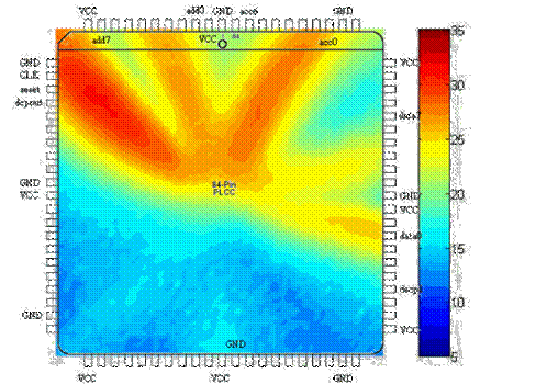
Thermal simulation tools are used to analyze heat distribution and identify hotspots. This helps optimize the design for efficient heat dissipation. - Gerber File Generation
Once the design is finalized, Gerber files are generated and sent to the PCB manufacturer for fabrication. - Testing and Validation
The fabricated Copper Base PCB is tested to ensure it meets the required performance and reliability standards.
Future Trends in Copper Base PCBs
As technology continues to evolve, several trends are shaping the future of Copper Base PCBs:
- Higher Power Density
The demand for higher power density in electronic devices will drive the need for more efficient thermal management solutions, such as Copper Base PCBs. - Advanced Materials
The development of advanced dielectric materials with higher thermal conductivity will further enhance the performance of Copper Base PCBs. - Integration with Advanced Technologies
Copper Base PCBs will play a key role in enabling emerging technologies such as electric vehicles, 5G networks, and renewable energy systems. - Sustainability
The electronics industry is increasingly focusing on sustainable practices, including the use of eco-friendly materials and energy-efficient designs for Copper Base PCBs.
Conclusio
Copper Base PCBs have become an essential component of modern electronics, offering superior thermal performance, reliability, and design flexibility. Their ability to efficiently dissipate heat makes them ideal for high-power applications such as LED lighting, power electronics, and automotive systems. As the demand for higher performance and compact designs continues to grow, Copper Base PCBs will remain at the forefront of innovation, enabling new possibilities and driving the development of next-generation electronic devices. By understanding the design considerations, advantages, and applications of Copper Base PCBs, engineers can leverage this technology to create reliable and high-performance solutions for the challenges of tomorrow.


