Copper Clad Board Manufacturing Expertise for PCB Production Demands

Key Takeaways
When navigating the complexities of PCB assembly, understanding the foundational elements of copper clad board manufacturing is critical These materials form the backbone of high-performance printed circuit boards, influencing everything from signal integrity to thermal dissipation Below, we break down the essential considerations for optimizing copper clad solutions in PCBA workflows
Core Considerations for Copper Clad Board Selection
1 Conductivity Optimization: The copper foil’s thickness and purity directly impact electrical performance For high-frequency PCBA applications, low-profile rolled copper (≤18 μm) minimizes signal loss
2 Thermal Management: Advanced dielectric materials like FR-4 Hybrid or polyimide blends balance heat resistance (up to 150°C) with mechanical stability
| Material Type | Thermal Conductivity (W/mK) | Typical Application |
|---|---|---|
| Standard FR-4 | 025 | Consumer Electronics |
| High-Tg FR-4 | 035 | Automotive Systems |
| Ceramic-Filled | 12 | RF/5G Infrastructure |
Tip: Always verify the glass transition temperature (Tg) of dielectric substrates to match your PCB assembly’s operational environment.
3 Signal Integrity Assurance: Tight impedance control (±5%) requires precise etching tolerances Laser-direct imaging (LDI) technology achieves trace widths under 25 μm, critical for high-density PCBA designs
Supplier Selection Criteria
When evaluating copper clad board manufacturers, prioritize partners with:
- ISO 9001/IATF 16949 certifications
- Real-time quality monitoring systems
- Prototyping-to-mass-production scalability
For PCBA projects demanding ultra-low loss (DF ≤0002), consider manufacturers specializing in hydrocarbon-based laminates These materials reduce dielectric loss by 40% compared to standard FR-4, though at a 15-20% cost premium
Process Innovations
Modern semi-additive fabrication (mSAP) techniques enable 3 μm copper traces, pushing the boundaries of miniaturization in PCB assembly Paired with automated optical inspection (AOI) systems, this ensures 50 ppm defect rates in volume production
By aligning material choices with PCBA requirements and leveraging cutting-edge manufacturing protocols, engineers can achieve optimal balance between performance, reliability, and cost-efficiency
Copper Clad Board Manufacturing Essentials Guide
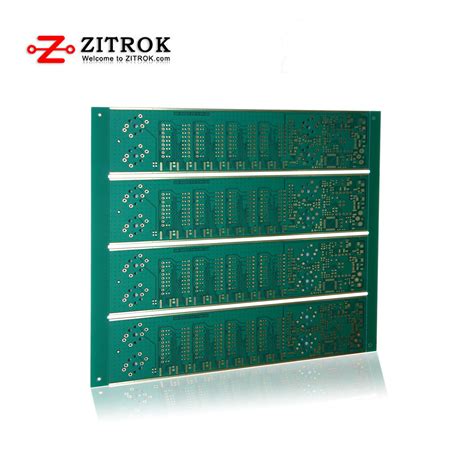
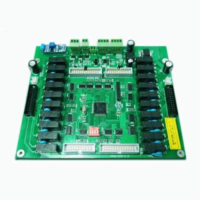
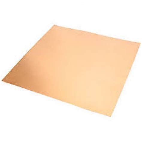
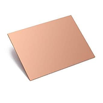
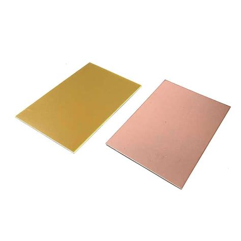
The foundation of reliable PCB assembly begins with mastering copper clad board manufacturing processes These specialized laminates, composed of conductive copper layers bonded to dielectric substrates, form the structural backbone of modern electronics Manufacturers prioritize material selection, balancing thermal expansion coefficients and dielectric constants to meet specific PCBA performance requirements
Critical production stages start with substrate preparation, where epoxy resins or polyimide films undergo precise thickness calibration Copper foil, typically ranging from ½ oz to 6 oz weights, is laminated under controlled heat (180–220°C) and pressure (300–500 PSI) to ensure void-free adhesion Advanced laser direct imaging (LDI) systems then etch circuit patterns with micron-level accuracy, maintaining impedance control for high-frequency PCB assembly applications
Drilling technologies have evolved to address miniaturization trends, with mechanical drills below 015mm diameter and laser ablation techniques creating microvias for multilayer PCBA designs Post-etching treatments like oxide coating or chemical roughening enhance copper surface adhesion for subsequent solder mask applications Quality assurance protocols mandate rigorous testing of peel strength (>10 N/mm) and thermal stress resistance (10+ cycles at 288°C), ensuring compatibility with lead-free soldering processes
Emerging innovations incorporate low-profile copper foils to reduce signal loss in 5G/mmWave circuits, while hybrid materials like ceramic-filled substrates address power electronics’ thermal management needs Manufacturers optimizing for PCB assembly efficiency now employ automated optical inspection (AOI) systems paired with real-time data analytics, achieving defect rates below 50 ppm across production batches
Understanding these manufacturing essentials enables engineers to specify appropriate glass transition temperature (Tg) grades and copper roughness parameters, directly impacting signal integrity in final PCBA implementations As IoT and automotive applications demand higher layer counts (12+ layers), manufacturers are adopting sequential lamination techniques and modified semi-additive processes (mSAP) to maintain dimensional stability across complex multilayer architectures
Advanced PCB Production Material Innovations
Recent advancements in PCB production materials are reshaping the landscape of modern electronics manufacturing Innovations in copper-clad laminate technology now prioritize not only electrical conductivity but also dimensional stability under extreme operating conditions Manufacturers are integrating high-purity electrolytic copper foils with ultra-low surface roughness, achieving signal transmission efficiencies critical for high-frequency applications like 5G infrastructure and automotive radar systems
A key breakthrough lies in the development of low-profile copper foils, which minimize skin effect losses while maintaining mechanical durability These materials are particularly vital for PCBA processes requiring fine-pitch traces, as they reduce the risk of micro-void formation during etching Concurrently, hybrid dielectric substrates combining polyimide with ceramic fillers are gaining traction, offering thermal expansion coefficients that align precisely with silicon-based components—a critical factor in minimizing solder joint stress during PCB assembly
Thermal management innovations are equally transformative Metal-core copper-clad boards embedded with thermally conductive prepregs now enable direct heat dissipation from power modules, reducing reliance on secondary cooling systems This advancement supports the growing demand for compact PCBA designs in aerospace and industrial automation, where space constraints coexist with high power density requirements
Material scientists are also addressing environmental sustainability through halogen-free flame-retardant laminates These meet stringent RoHS directives without compromising dielectric strength—a non-negotiable trait for high-voltage applications like EV charging systems
The synergy between material science and PCB assembly workflows is further evident in the adoption of laser-direct structuring (LDS) compatible substrates These allow for three-dimensional circuit integration, streamlining production for complex PCBA geometries in wearable tech and medical devices
As industry standards evolve, manufacturers are leveraging AI-driven analytics to validate material performance across thermal cycling and humidity tests This data-centric approach ensures that next-generation copper-clad boards meet signal integrity benchmarks even in multi-layered, high-speed digital designs—bridging the gap between prototyping and mass production scalability
Optimizing Conductivity in Copper Clad Designs
Achieving optimal conductivity in copper clad boards requires a meticulous balance of material selection, surface treatment, and geometric precision Critical factors such as copper foil thickness, surface roughness, and dielectric properties directly influence electrical performance in PCB assembly applications Manufacturers prioritize ultra-low profile copper foils (≤12 μm) to minimize signal loss while maintaining mechanical durability, particularly in high-frequency PCBA designs
Advanced etching techniques, including differential and additive processing, enable precise control over conductor width and spacing This ensures consistent impedance matching—a non-negotiable requirement for modern high-speed circuits The implementation of reverse-treated copper foils reduces peak surface roughness by 40-60%, significantly lowering insertion loss in 5G and IoT applications
Thermal dynamics play an underappreciated role in conductivity optimization Copper clad board producers now integrate thermal conductivity enhancers like ceramic-filled substrates, which dissipate heat 25% faster than standard FR-4 materials without compromising dielectric stability This dual functionality proves vital in power electronics and automotive PCB assembly, where thermal cycling endurance directly impacts long-term conductivity
Signal integrity specialists emphasize the importance of cross-sectional uniformity in multilayer designs Automated optical inspection (AOI) systems verify copper distribution accuracy to ±2% tolerance, preventing current crowding in high-density interconnect (HDI) PCBA configurations Recent advancements in plasma surface activation further improve copper-to-substrate adhesion, reducing micro-void formation by 30% during thermal stress tests
Leading manufacturers align their processes with IPC-4562A standards, employing real-time resistance monitoring systems during lamination This proactive quality control approach ensures bulk conductivity remains within 05% of design specifications across production batches—a critical metric for aerospace and medical-grade PCB assembly applications requiring mission-critical reliability
Thermal Management Solutions for PCBs Explained
Effective thermal management remains a cornerstone of reliable PCB assembly, particularly in high-power applications where heat dissipation directly impacts performance and longevity Modern manufacturers employ precision-engineered copper-clad laminates with optimized thickness ratios to balance conductivity and thermal resistance These materials work synergistically with advanced cooling architectures, such as embedded thermal vias and strategically placed heatsinks, to redirect thermal energy away from sensitive components
In PCBA processes, the integration of thermally conductive dielectric layers—often reinforced with ceramic fillers or graphene-based composites—enhances heat distribution across the board This approach minimizes localized hotspots that could compromise signal integrity or accelerate component degradation For mission-critical systems, engineers increasingly adopt active cooling solutions like microfluidic channels, which operate in tandem with the copper substrate’s innate thermal conductivity to maintain operational temperatures within safe thresholds
Material selection plays a pivotal role, with high-Tg (glass transition temperature) laminates and metal-core substrates becoming standard for applications demanding rigorous thermal cycling resilience During PCB assembly, manufacturers leverage infrared thermal imaging to validate heat dissipation patterns, ensuring compliance with industry benchmarks such as IPC-2221 This quality-driven methodology not only extends product lifespans but also reduces failure rates in environments subjected to extreme temperature fluctuations
As miniaturization trends intensify, the interplay between copper weight, layer stackup design, and surface finishes grows more nuanced Progressive PCBA providers now implement simulation-driven layouts, using finite element analysis to predict thermal behavior before prototyping This proactive stance enables the development of boards capable of sustaining optimal performance in aerospace, automotive, and 5G infrastructure applications where thermal management directly correlates with system reliability
Signal Integrity Assurance in Circuit Board Fabrication
Maintaining signal integrity remains a critical challenge in modern high-frequency and high-speed PCB assembly applications As data transmission rates exceed GHz ranges, even minor inconsistencies in copper clad board (CCB) properties can lead to signal distortion, timing errors, or electromagnetic interference (EMI) Leading PCBA manufacturers address these challenges through three core strategies: impedance control, material optimization, and advanced fabrication techniques
Precision etching processes achieve controlled impedance by maintaining ±5% tolerance in conductor width and spacing, crucial for matching transmission line characteristics with signal frequencies High-performance CCB substrates with stable dielectric constants (Dk values between 35-45 at 1 GHz) minimize signal phase variations across temperature fluctuations For multilayer designs, manufacturers implement ground plane optimization and differential pair routing to reduce crosstalk below -40 dB in pcb assembly configurations
Advanced pcba solutions now incorporate hybrid materials like low-loss PTFE composites or ceramic-filled laminates, achieving dissipation factors (Df) as low as 0002 at 10 GHz These materials work synergistically with surface finish technologies such as immersion silver or ENIG (Electroless Nickel Immersion Gold) to maintain consistent signal paths Real-time eye diagram analysis during prototype testing validates signal quality metrics, including jitter performance below 1 ps RMS in 56 Gbps applications
Thermo-mechanical simulations further ensure that coefficient of thermal expansion (CTE) mismatches between copper and substrate materials don’t compromise signal paths during thermal cycling This multilayered approach enables CCB manufacturers to deliver 05 dB/inch insertion loss at 28 GHz frequencies, meeting stringent requirements for 5G infrastructure and automotive radar systems
Selecting Trusted Copper Clad Board Suppliers
Identifying reliable copper clad board manufacturers requires a systematic approach that balances technical expertise, material quality, and supply chain reliability As PCB assembly processes grow more complex, the choice of base materials directly impacts signal integrity, thermal performance, and long-term durability of end products Leading suppliers distinguish themselves through certifications such as IPC-4101 for material consistency and UL 94 flammability ratings, ensuring compliance with global safety standards
When evaluating potential partners, prioritize manufacturers with proven experience in high-frequency and high-speed PCB applications, particularly for advanced PCBA projects Transparent documentation of dielectric constant (Dk) and dissipation factor (Df) values is critical, as these parameters influence impedance control in multi-layer designs Additionally, assess their capability to provide low-loss laminates for 5G infrastructure or automotive electronics, where thermal management and conductivity optimization are non-negotiable
Supply chain resilience is another key consideration Top-tier suppliers maintain rigorous raw material traceability systems, reducing risks of contamination or batch inconsistencies Look for partnerships with copper foil producers and resin suppliers that adhere to RoHS and REACH directives, especially for applications requiring environmental compliance
For prototyping or high-volume PCB assembly, verify the manufacturer’s capacity for customization—such as adjusting copper weight (e.g., 1 oz to 3 oz) or offering hybrid materials like FR-4 with polyimide blends Real-time technical support during design-for-manufacturing (DFM) stages further ensures seamless integration of copper clad boards into your PCBA workflow
Finally, analyze supplier track records through client testimonials and case studies Manufacturers with documented success in aerospace, medical devices, or IoT hardware often demonstrate superior problem-solving capabilities for niche requirements By aligning supplier capabilities with your project’s signal integrity goals and thermal reliability thresholds, you establish a foundation for scalable, high-performance electronics manufacturing
Precision-Engineered Copper Clad Manufacturing Processes
Modern PCB assembly relies on copper clad laminates engineered with micron-level accuracy to meet the exacting demands of high-frequency and high-density circuit designs At the core of these processes lies advanced lamination technology, where dielectric substrates are bonded with copper foil under precisely controlled temperature and pressure conditions This ensures uniform thickness and eliminates voids, critical for maintaining signal integrity in multi-layer PCBA applications
State-of-the-art etching techniques further refine copper patterns, achieving trace widths as narrow as 25µm while preserving edge definition Manufacturers employ automated optical inspection (AOI) systems to validate dimensional tolerances, a step that directly impacts thermal management capabilities in high-power boards For PCB assembly workflows requiring impedance control, laser-drilled microvias and plasma-treated surfaces enhance plating adhesion, reducing signal loss in RF and microwave applications
Material selection plays an equally vital role High-Tg (glass transition temperature) resins paired with low-profile copper foils mitigate thermal expansion mismatches—a common failure point in PCBA subjected to thermal cycling Leading suppliers now integrate real-time process monitoring, leveraging AI-driven analytics to adjust parameters like pressurization rates or curing times dynamically
These precision-driven methods not only improve conductivity but also enable thinner, lighter boards without compromising durability—a key requirement for aerospace and medical-grade electronics By aligning manufacturing protocols with IPC-4101 and MIL-PRF-31032 standards, producers ensure compatibility with automated PCB assembly lines, where consistency across batches is non-negotiable
The interplay between material science and process innovation continues to redefine performance benchmarks, making precision engineering not just a manufacturing phase but the foundation of reliable, next-generation circuit fabrication
Industry-Standard PCB Material Quality Criteria
Modern PCB assembly relies on stringent material quality benchmarks to ensure reliability across demanding applications At the core of these standards lies the evaluation of base material properties, including dielectric strength, thermal stability, and copper foil adhesion For PCBA processes, laminates must meet IPC-4101 specifications, which define acceptable ranges for critical parameters such as glass transition temperature (Tg) and dielectric constant (Dk) These metrics directly influence signal integrity, especially in high-frequency or high-power designs where impedance control is non-negotiable
Third-party certifications like UL 94 flammability ratings and RoHS compliance further validate material suitability Manufacturers prioritize substrates with low z-axis expansion coefficients to prevent delamination during thermal cycling—a common failure point in multilayer boards Advanced copper clad board producers employ automated optical inspection (AOI) systems to detect microvoids or uneven etching, ensuring consistent copper thickness tolerances within ±5% This precision minimizes insertion losses in RF applications and supports fine-pitch PCB assembly requirements
The interplay between material selection and PCBA performance extends to environmental resilience Industrial-grade boards, for instance, demand materials with moisture absorption rates below 01% to maintain insulation resistance in humid conditions Leading suppliers now integrate real-time traceability systems, linking batch-specific test reports to ISO 9001 quality management protocols By aligning with these industry benchmarks, engineers mitigate risks in prototyping and scale-up phases while achieving mean time between failures (MTBF) targets exceeding 100,000 hours in mission-critical systems
Conclusion
As the foundation of modern electronics, copper clad board manufacturing remains critical to meeting evolving PCB assembly requirements The interplay between material science, precision engineering, and stringent quality controls ensures that high-frequency applications and miniaturized designs achieve optimal performance By prioritizing conductivity, thermal stability, and signal integrity, manufacturers deliver substrates that align with the rigorous demands of PCBA workflows, where even minor deviations can compromise end-product reliability
Selecting a trusted partner requires evaluating adherence to industry certifications and the ability to innovate alongside emerging technologies like 5G and IoT Advanced copper clad boards must not only support efficient PCB assembly processes but also withstand stressors such as thermal cycling and mechanical strain This dual focus on material excellence and manufacturability underscores why collaboration with specialized producers is vital for achieving first-pass yield targets in PCBA production
Ultimately, the convergence of cutting-edge metallization techniques and data-driven process optimization defines success in this field As circuit densities increase and global standards tighten, manufacturers that invest in ultra-low-loss laminates and controlled impedance materials will remain indispensable to electronics innovators The journey from raw materials to functional PCBA underscores the irreplaceable role of precision-engineered copper clad solutions in powering tomorrow’s technological breakthroughs

Frequently Asked Questions
What distinguishes high-quality copper clad boards in PCB manufacturing?
Superior copper clad boards exhibit optimal conductivity and thermal stability, ensuring reliable performance in high-frequency applications Key factors include copper foil purity (≥999%), dielectric constant consistency, and adherence to IPC-4101 standards for material grading
How do thermal management solutions enhance PCB longevity?
Advanced thermal management integrates metal-core substrates and thermally conductive prepregs, effectively dissipating heat from components like power transistors and LED arrays This reduces thermal stress, minimizing delamination risks during PCBA processes
Why is signal integrity critical in modern PCB designs?
With rising high-speed signal demands (e.g., 5G, IoT), impedance control and low-loss dielectrics become essential Precision etching of copper traces and stringent surface roughness controls (05μm) mitigate signal distortion in RF PCBA applications
What criteria define trusted copper clad board suppliers?
Reputable manufacturers provide UL-certified materials, ISO 9001-compliant workflows, and 24/7 technical support Transparent lead time guarantees and RoHS compliance further validate supplier reliability for mission-critical PCB assembly projects
How does PCBA integration impact copper clad board selection?
Compatibility with reflow soldering profiles and CTE (Coefficient of Thermal Expansion) matching are vital Boards must withstand multiple thermal cycles during SMT assembly without warping, ensuring seamless integration with mixed-technology PCBA workflows
Explore Professional PCB Assembly Solutions
For tailored PCB assembly and PCBA services that align with your copper clad board specifications, please click here to consult our engineering team