Copper Foil Current Carrying Capacity in PCBs: A Comprehensive Analysis
Abstract
The current carrying capacity of copper foil in printed circuit boards (PCBs) is a critical factor in ensuring reliable performance, thermal management, and long-term durability of electronic devices. This paper explores the key factors influencing copper foil current carrying capacity, including trace width, thickness, temperature rise, and environmental conditions. Additionally, it discusses industry standards, calculation methods, and design considerations to optimize PCB performance. The findings provide valuable insights for PCB designers and engineers to enhance current handling capabilities while minimizing overheating risks.
1. Introduction
Printed Circuit Boards (PCBs) serve as the backbone of modern electronics, providing electrical connections between components. Copper foil, the primary conductive material in PCBs, must efficiently carry current without excessive resistive heating. The current carrying capacity of copper traces depends on multiple factors, such as cross-sectional area, ambient temperature, and thermal dissipation.
Understanding copper foil current carrying capacity is essential for preventing trace failures, voltage drops, and thermal damage. This paper examines the principles, calculations, and best practices for determining safe current limits in PCB designs.
2. Factors Affecting Copper Foil Current Carrying Capacity
2.1 Trace Width and Thickness
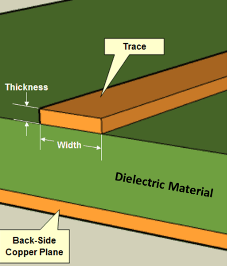
The current carrying capacity of a copper trace is directly proportional to its cross-sectional area. Wider and thicker traces can handle higher currents due to lower resistance. The relationship is expressed as:
[ R = \rho \frac{L}{A} ]
Where:
- ( R ) = Resistance (Ω)
- ( \rho ) = Resistivity of copper (( 1.68 \times 10^{-8} \, \Omega \cdot m ))
- ( L ) = Trace length (m)
- ( A ) = Cross-sectional area (( width \times thickness ))
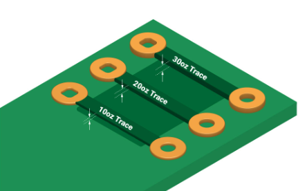
Standard copper thicknesses include:
- 1 oz/ft² (35 µm) – Common in consumer electronics
- 2 oz/ft² (70 µm) – Used in high-current applications
- 3 oz/ft² (105 µm) and above – For power electronics
2.2 Temperature Rise and Derating
Excessive current causes resistive heating, leading to temperature rise. The IPC-2152 standard provides guidelines for current vs. temperature rise based on trace dimensions.
Key considerations:
- 10°C Rise – Conservative design (long lifespan)
- 20°C Rise – Balanced performance
- 50°C+ Rise – High-power applications (requires thermal management)
Derating is necessary in high-temperature environments to prevent overheating.
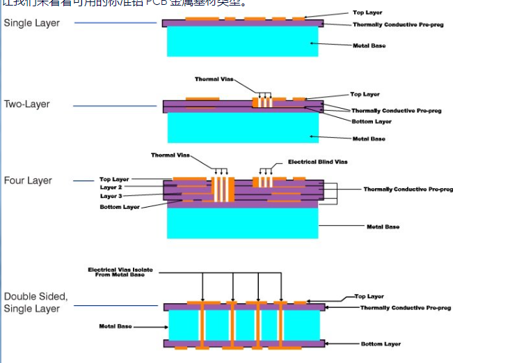
2.3 PCB Material and Thermal Conductivity
The substrate material (e.g., FR-4, metal-core PCBs) affects heat dissipation. FR-4 has limited thermal conductivity (~0.3 W/m·K), while metal-core PCBs (e.g., aluminum) offer better heat transfer.
2.4 Ambient Conditions and Airflow
Natural convection, forced airflow, and enclosure design influence cooling. Traces in enclosed spaces require lower current ratings than those in ventilated environments.
3. Current Carrying Capacity Calculation Methods
3.1 IPC-2152 Standard
The IPC-2152 standard provides empirical data for current vs. trace width, thickness, and temperature rise. Designers use lookup tables or software tools to determine safe current limits.
Example:
- 10°C Rise, 1 oz Cu, 10 mm width → ~5 A
- 20°C Rise, 2 oz Cu, 10 mm width → ~10 A
3.2 Empirical Formulas
For quick estimates, modified versions of the “I = k·ΔT^0.44·A^0.725” formula (from IPC-2221) are used, where:
- ( I ) = Current (A)
- ( k ) = Constant (0.024 for external traces, 0.048 for internal)
- ( ΔT ) = Temperature rise (°C)
- ( A ) = Cross-sectional area (mil²)
3.3 Simulation and Finite Element Analysis (FEA)
Advanced PCB design tools (e.g., ANSYS, Cadence) simulate current density and thermal behavior, providing precise predictions for complex layouts.
4. Design Considerations for High-Current PCBs
4.1 Increasing Trace Width and Thickness
- Use wider traces for high-current paths.
- Consider thicker copper (2 oz or more) for power circuits.
4.2 Thermal Relief and Heat Sinking
- Use thermal vias to dissipate heat to inner layers or heatsinks.
- Implement copper pours for better heat distribution.
4.3 Multi-Layer PCBs for Current Sharing
- Parallel traces on multiple layers reduce resistance and improve current handling.
4.4 Avoiding Sharp Corners and Narrowing Traces
- Sharp bends increase current crowding, leading to hotspots.
- Use curved or 45° angles for smooth current flow.
5. Practical Applications and Case Studies
5.1 Power Electronics (DC-DC Converters, Motor Drives)
High-current traces in power electronics require careful thermal management. Thick copper (3 oz+) and thermal vias are commonly used.
5.2 Automotive PCBs
Automotive PCBs must handle high currents while withstanding vibration and temperature extremes. Reinforced copper and robust thermal designs are critical.
5.3 High-Frequency PCBs (RF Applications)
Skin effect at high frequencies reduces effective conduction depth. Wider traces and surface treatments mitigate losses.
6. Conclusion
The current carrying capacity of PCB copper foil is a fundamental aspect of reliable electronic design. By considering trace geometry, temperature rise, and thermal management, engineers can optimize PCB performance for various applications. Adherence to IPC standards, simulation tools, and best practices ensures safe and efficient current handling.
Future advancements in PCB materials (e.g., high-thermal-conductivity substrates) and manufacturing techniques (embedded cooling) will further enhance current capacity in next-generation electronics.