copper in pcb
1. Understanding copper foil in PCBs
Copper foil used in the PCB industry is more complex than you might think. Copper is both an excellent conductor and an excellent thermal conductor, making it an ideal conductor for most PCB applications.
Copper foil has many other properties that are important for engineers to understand.
Copper foil used in the PCB industry is generally rolled annealed copper (RA) or electrolytic (ED). The manufacturing process of rolled copper foil starts with a pure copper billet, which is continuously rolled and reduced to the desired thickness.
ED copper foil is manufactured using an electroplating process, in which copper is plated on a rotating titanium drum, and as the drum rotates, copper ions are gradually deposited to form the copper foil.
The rotation speed of the titanium drum directly affects the thickness of the copper foil. After the copper foil is made, both RA and ED copper foils need to go through multiple process treatments.

GET PCB MANUFACTURING AND ASSEMBLY QUOTE NOW!
2. Treatment of copper foil
Copper foil has a variety of treatments for a variety of reasons. Some of these treatments are passivation treatments, which are designed to ensure that the copper foil does not oxidize before use.
Other copper foil treatments are designed to enhance good chemical adhesion to certain resin systems (e.g. PPE vs. PTFE). Due to differences in resin systems, the material will react differently to various treatments.
Because each resin system has different bonding characteristics, some treatment/resin combinations will work better than others for good adhesion. There are also copper foil treatments that ensure proper bonding at high temperatures.
There are also other treatments that provide a reliable bonding surface to ensure long-term reliability at high temperatures, etc.
For rigid PCB applications, ED copper foil is the most common, but RA copper foil is also used. Generally speaking, RA copper foil is more expensive than ED copper foil.
RA copper foil is generally not used unless some of its characteristics are more advantageous for the application. The manufacturing process of RA copper foil makes it have a very smooth surface, and smooth copper foil has lower insertion loss, so it is well suited for high-frequency and ultra-high-speed digital applications.
As a product of a unique manufacturing process for copper foil, RA copper foil also has an in-plane crystalline structure, which is very beneficial for applications that require circuit bending. Correspondingly, RA copper foil has a technical drawback related to this crystal structure, namely the etching of tiny circuit features. Of course, this problem can be overcome to some extent using specific etching of RA copper foil.
ED copper foil is widely used throughout the PCB industry. There are many different types of ED copper foil, which are usually classified by surface roughness and/or treatment. IPC classifies ED copper foil into different categories based on copper foil roughness, including LP (low profile), VLP (very low profile) and HVLP (very low profile).
GET PCB AND ASSEMBLY SERVICE QUOTE NOW!
3. There are many ways to measure copper foil roughness
There are many ways to measure copper foil roughness, and the measurement results can be confusing due to differences in methods. Generally speaking, there are two roughness measurement methods: contact measurement and non-contact measurement.
Contact measurement uses a physical probe (i.e., a stylus) to measure the peaks and valleys on the copper foil surface. Non-contact measurement generally determines the peaks and valleys on the copper foil surface through reflected light or laser measurement.
Due to the different sizes of the stylus tip, the accuracy of contact profilometers is low and cannot detect the depth of ultra-narrow roughness valleys. Furthermore, the stylus may only “plow” over the highest point, but it cannot achieve accurate measurement.
Experienced engineers are familiar with these problems and can often make some minor adjustments to alleviate accuracy issues. But in general, for fine-grained copper foil, non-contact profilometers are usually more accurate than contact profilometers.
There are many ways to describe the surface roughness characteristics of copper foil
There are many ways to describe the surface roughness characteristics of copper foil. PCB manufacturing engineers usually use Rz values to describe, Rz represents the peak-to-valley value measured on multiple straight lines on a sample area. If the Rz value is measured as an area (rather than a straight line), then Rz will be named Sz.
The Sz value has the same meaning as the Rz value. For high-frequency or high-speed digital (HSD) design engineers, the Rq or Sq parameter value of copper foil is usually required. Rq/Sq represents the root mean square value of the copper foil surface roughness measured on multiple samples.
Through the classic electromagnetic model, it is found that the Rq/Sq parameter can better reflect the impact of copper foil roughness on RF or HSD performance, and its electromagnetic model can better match the performance of actual circuits.
There is another characteristic description of the surface roughness of copper foil that is of interest in modeling: the surface area index (SAI), also known as the surface area ratio. It is defined as the ratio of the surface area of the roughness in the scanned area to the area of the ideal flatness in the area.
This roughness value can be used for specific electromagnetic model simulations, so that the simulation results can show excellent matching and accuracy with the actual circuit over an ultra-wide bandwidth.

4. Wide application of copper in power electronics
For power semiconductor devices, silicon is the most common element, but due to its high conductivity, copper is the best choice for substrates on printed circuit boards (PCBs) and ceramic substrates.
Due to its thermal conductivity, copper has become the most commonly used material for substrates and heat sinks. In addition, copper is very important for the metallization and interconnection of power devices.
The increasing energy density, current carrying capacity and reliability requirements are also the reasons why copper is widely used in this industry. Copper has the following advantages: easy availability, relatively cheap, and stable supply.
(1) Comparison of copper and aluminum
Depending on the specific application, aluminum is the best substitute for copper. For example, in heat sinks, aluminum is cheaper and lighter than copper, so aluminum is the preferred material.
However, for certain applications where thermal conductivity is more important than weight reduction, copper is a more ideal material. At room temperature, copper has a thermal conductivity of 400 W/m-K, while aluminum has a thermal conductivity of 235 W/m-K. Therefore, all other factors being equal, copper heat sinks are better at dissipating heat than aluminum heat sinks.
As a result, many power modules with integrated copper spoiler heat sinks are now market-proven and successfully used in hybrid and electric vehicles.
Aluminum and aluminum alloys are widely used for chip metallization. They have low electrical resistance and good adhesion to silicon and silicon oxide layers. Nevertheless, copper metallization has been introduced in the chip field to replace aluminum metallization due to its better thermal and current conductivity.
The lower resistivity allows for higher current per unit area and less heat per unit current, and the higher thermal conductivity allows for more effective heat dissipation. These two obvious advantages allow copper to have higher current and better compactness.
The downside is that copper is not as easy to etch as aluminum in the dry etching process. Therefore, not all chips are treated with copper metallization. Furthermore, due to cost and stress issues, copper metallization thickness can only be between 5 μm and 10 μm, but thicker layers provide greater current drive capability, higher thermal capacity and heat dissipation.
Although, there may be some workarounds, such as Danfoss’s bond buffer technology, which fuses a thin copper foil to the top of the chip.
Another driver for the use of copper for standard chip metallization is reliability. The main cause of failure in state-of-the-art power modules is bond wire detachment. Therefore, new solutions have been developed to interconnect multiple chips to power modules instead of traditional aluminum wires.
Many solutions rely on copper materials of different shapes and geometries: copper wires, copper ribbons, copper pillars, copper quick-connects or copper frames, which can be soldered, sintered or welded to the chip.
Other solutions include planar interconnects and chip embedding technologies, in which the top electrode contacts are connected by copper vias.
(2) Heavy copper is no longer heavy enough
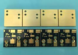
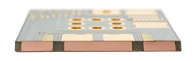
Although some substrates still use aluminum metallization, copper is the main material used for PCB inner and outer layer conductors and ceramic substrates.
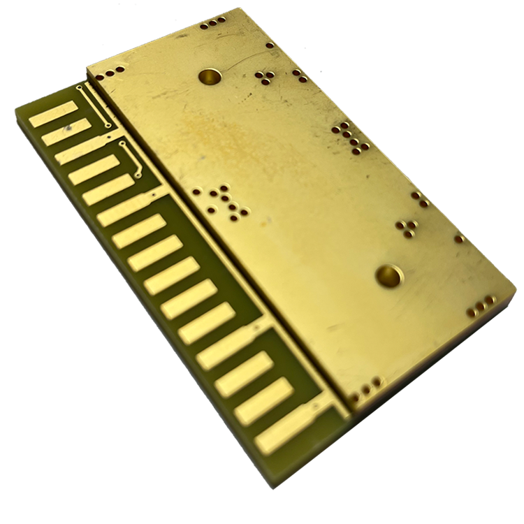
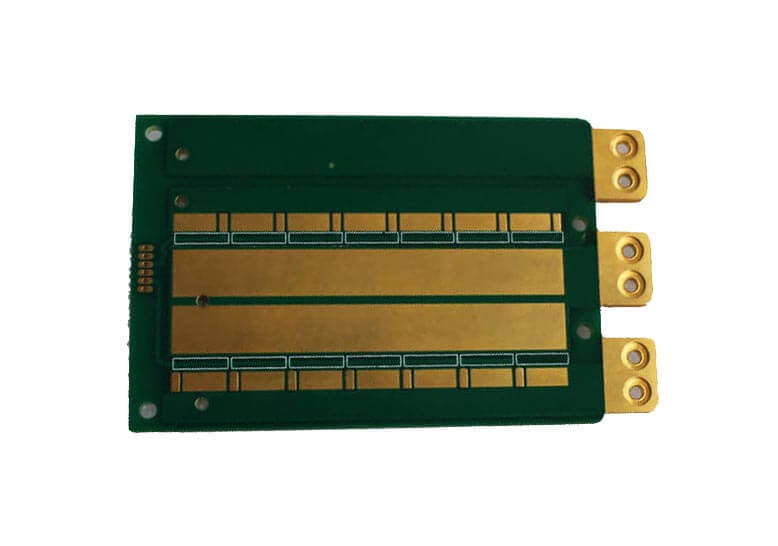
Copper thickness can be specified as the weight of copper per square foot in ounces (oz/ft2). The most common PCBs on the market are manufactured for low-power applications, with copper conductors made of copper weighing no less than 0.5 oz/ft2 (18 μm) and no more than 3 oz/ft2 (105 μm).
For high-power applications, thick copper circuits can be made with copper weighing between 4 oz/ft2 (140 μm) and 20 oz/ft2 (686 μm). Copper weights exceeding 20 oz/ft2 are also possible, and this is called extreme copper.
In particular, direct bond copper (DBC) and active metal brazing (AMB) substrates are used to mount multiple power devices in parallel on a module to achieve the power rating required by the specified application. Such substrates are available with copper thicknesses from 127 μm to 800 μm.
However, there is also a real trend towards miniaturization of power modules. As a result, module manufacturers are increasingly placing increasing demands on semiconductor and packaging technologies in order to further increase the output power of existing or smaller component packages.
Furthermore, since the performance increase should not affect cost and reliability, the substrate and baseplate or heat sink must be connected using new technologies or preferably integrated into one assembly. This ultimately led to the development of substrates with copper layers thicker than 1 mm.
Typically, thick copper layers are produced using the same wet chemical etching process as standard copper layers. Due to its isotropic characteristics, wet chemical etching is not suitable for thick copper layers, which would otherwise result in larger trenches between the wires, while customers require narrower trenches to reduce the module package size.
Therefore, special construction technologies must be developed to achieve small gaps, straight sidewalls and negligible bottom incision.