Crazing in Printed Circuit Boards (PCBs): Causes, Effects, and Mitigation Strategies
Introduction
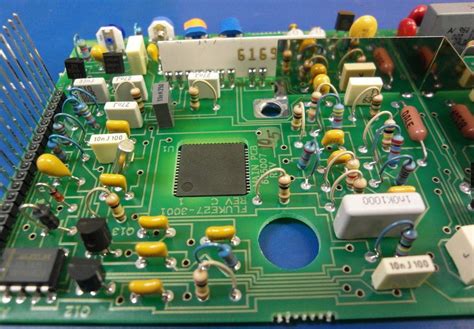
Printed Circuit Boards (PCBs) are the backbone of modern electronics, providing mechanical support and electrical connections for components. However, PCBs are susceptible to various forms of degradation, one of which is crazing. Crazing refers to the formation of fine cracks or micro-fractures in the substrate material, typically the epoxy resin or solder mask layer. These cracks can compromise the structural integrity and electrical performance of the PCB, leading to potential failures in electronic devices.
This article explores the phenomenon of crazing in PCBs, including its causes, effects, detection methods, and mitigation strategies.
1. What is Crazing in PCBs?
Crazing is a type of surface defect characterized by a network of tiny cracks that develop in the polymer-based materials used in PCBs, such as:
- Solder mask layers
- Epoxy resin substrates
- Conformal coatings
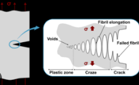
Unlike major cracks that lead to immediate failure, crazing consists of microscopic fissures that may initially appear harmless but can propagate over time due to thermal cycling, mechanical stress, or environmental exposure.
Key Characteristics of Crazing:
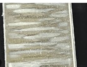
- Fine, web-like cracks visible under magnification
- Often starts at stress concentration points (e.g., edges, drilled holes)
- May not immediately affect electrical performance but can worsen with time
2. Causes of Crazing in PCBs
Several factors contribute to the development of crazing in PCBs:
A. Thermal Stress
- Thermal cycling: Repeated heating and cooling during operation can cause expansion and contraction, leading to micro-cracks.
- High-temperature soldering: Excessive heat during assembly can weaken the solder mask or substrate.
B. Mechanical Stress
- Bending or flexing: Improper handling or flexing of rigid PCBs can induce stress.
- Vibration and shock: Mechanical vibrations in industrial or automotive applications can accelerate crazing.
C. Environmental Factors
- Moisture absorption: Hydroscopic materials (e.g., FR-4) absorb moisture, which expands when heated, causing internal stress.
- Chemical exposure: Harsh chemicals (solvents, cleaning agents) can degrade polymer layers.
D. Material Defects
- Poor-quality solder mask: Low-grade resins are more prone to cracking.
- Inadequate curing: Improper UV or thermal curing of solder mask can leave it brittle.
E. Manufacturing Process Issues
- Over-etching: Aggressive etching processes can weaken the substrate.
- Improper lamination: Poor adhesion between layers can lead to delamination and crazing.
3. Effects of Crazing on PCB Performance
While crazing may not cause immediate failure, its long-term effects can be detrimental:
A. Electrical Failures
- Conductive pathways: Cracks can expose copper traces, leading to short circuits.
- Increased resistance: Micro-cracks in conductive layers can disrupt signal integrity.
B. Reduced Mechanical Strength
- Delamination risk: Crazing can propagate into deeper layers, causing separation.
- Fracture susceptibility: Stressed areas may develop full cracks under load.
C. Corrosion and Contamination
- Moisture ingress: Cracks allow humidity and contaminants to penetrate, accelerating corrosion.
- Dendritic growth: Ionic contaminants can form conductive filaments, causing leakage currents.
D. Aesthetic and Quality Concerns
- Cosmetic defects: Visible crazing may lead to rejection in high-reliability applications.
- Warranty and reliability issues: Premature failures can increase repair costs.
4. Detection and Inspection Methods
Early detection of crazing is crucial to prevent catastrophic failures. Common inspection techniques include:
A. Visual Inspection (Magnification)
- Optical microscopes (10x–50x magnification) can reveal surface-level crazing.
- Digital microscopes with image analysis software help in documentation.
B. Cross-Sectional Analysis
- Cutting and polishing PCB samples to examine internal cracks under a microscope.
C. Scanning Electron Microscopy (SEM)
- High-resolution imaging to detect nano-scale cracks.
D. Dye Penetration Testing
- Applying a colored dye that seeps into cracks, making them visible under UV light.
E. Acoustic Microscopy
- Ultrasonic imaging to detect subsurface defects without destructive testing.
5. Mitigation and Prevention Strategies
To minimize the risk of crazing, PCB manufacturers and designers can adopt the following best practices:
A. Material Selection
- High-Tg (Glass Transition Temperature) substrates: More resistant to thermal stress.
- Flexible solder masks: Polyimide-based masks are less prone to cracking.
B. Improved Manufacturing Processes
- Controlled lamination: Ensuring proper adhesion between layers.
- Optimized curing: Proper UV/thermal curing of solder masks to avoid brittleness.
C. Design Considerations
- Avoid sharp corners: Rounded traces reduce stress concentration.
- Proper via placement: Minimizing mechanical stress around drilled holes.
D. Environmental Protection
- Conformal coatings: Silicone or acrylic coatings protect against moisture and chemicals.
- Hermetic sealing: For high-reliability applications (e.g., aerospace, medical).
E. Stress Testing and Quality Control
- Thermal cycling tests: Simulating operating conditions to detect early crazing.
- Mechanical bend tests: Ensuring flexibility without cracking.
6. Case Studies: Crazing-Related Failures
A. Automotive Electronics
- Issue: Crazing in engine control unit (ECU) PCBs due to thermal cycling.
- Solution: Switching to high-Tg materials and improved conformal coatings.
B. Consumer Electronics
- Issue: Solder mask crazing in smartphones after repeated drop tests.
- Solution: Using flexible solder masks and reinforced PCB edges.
C. Industrial PCBs
- Issue: Moisture-induced crazing in outdoor equipment.
- Solution: Implementing hydrophobic coatings and hermetic sealing.
7. Future Trends in PCB Durability
Advancements in PCB materials and manufacturing aim to reduce crazing risks:
- Nanocomposite resins: Enhanced crack resistance.
- 3D-printed PCBs: Reduced stress points through additive manufacturing.
- Self-healing coatings: Polymers that repair micro-cracks autonomously.
Conclusion
Crazing in PCBs is a critical reliability concern that can lead to long-term failures if not addressed. By understanding its causes, effects, and detection methods, manufacturers can implement preventive measures such as material improvements, optimized designs, and rigorous testing. As electronics continue to evolve, advancements in PCB technology will further mitigate crazing risks, ensuring longer-lasting and more reliable devices.
Key Takeaways:
- Crazing is caused by thermal, mechanical, and environmental stresses.
- Early detection through microscopy and testing prevents failures.
- Mitigation involves material selection, design optimization, and protective coatings.
- Future innovations (self-healing coatings, nanocomposites) will enhance PCB durability.
By proactively addressing crazing, the electronics industry can improve product lifespan and performance in demanding applications.