Critical Factors for Success and Failure in PCB Design
Introduction
Printed Circuit Board (PCB) design represents one of the most crucial stages in electronic product development, serving as the physical foundation that brings electronic concepts to life. The quality of PCB design directly impacts product performance, reliability, manufacturing yield, and ultimately the commercial success of the final product. In today’s competitive electronics market where devices are becoming increasingly complex while expected to be smaller, faster, and more reliable, understanding the key factors that determine PCB design success or failure has never been more important.
This article examines the critical considerations that separate successful PCB designs from problematic ones. We will explore fundamental design principles, common pitfalls, and best practices across various aspects of PCB development—from initial schematic capture to final manufacturing output. By understanding these factors, engineers can avoid costly mistakes, reduce design iterations, and create PCBs that meet all functional requirements while being manufacturable, reliable, and cost-effective.

1. Proper Schematic Design and Documentation
The foundation of any successful PCB design lies in a well-constructed schematic. Many design failures can be traced back to schematic-level issues that weren’t properly addressed before layout began.
1.1 Schematic Accuracy and Completeness
A complete and accurate schematic serves as the single source of truth for the entire design. Common schematic-related failures include:
- Incorrect or missing connections
- Wrong component symbols or footprints
- Incomplete power and ground networks
- Missing bypass capacitors or pull-up/pull-down resistors
- Improper net labeling that causes connectivity errors
Best practices include:
- Using a standardized symbol library with verified components
- Implementing thorough design rule checks (DRC) at schematic stage
- Clearly labeling all nets, especially critical signals
- Including all necessary power and ground connections
- Adding comprehensive notes about special requirements
1.2 Design Hierarchy and Organization
For complex designs, proper schematic organization becomes critical:
- Modularize the design into functional blocks
- Use hierarchical sheets when appropriate
- Maintain consistent naming conventions
- Clearly document interfaces between modules
Poor schematic organization leads to confusion during layout and makes design reviews more difficult, increasing the chance of errors being overlooked.
2. Component Selection and Management
Component selection decisions made early in the design process have far-reaching consequences for manufacturability, reliability, and cost.
2.1 Component Availability and Lifecycle
Design failures often occur when:
- Selecting components that are obsolete or nearing end-of-life
- Choosing parts with long lead times or allocation periods
- Relying on single-source components without alternatives
- Using components that will be discontinued during product lifecycle
Best practices include:
- Checking component availability across multiple distributors
- Reviewing manufacturer lifecycle status
- Identifying acceptable alternates for critical components
- Considering second-source options for key parts
2.2 Footprint and Package Considerations
Incorrect footprints account for numerous PCB failures:
- Using outdated or incorrect footprint libraries
- Not accounting for manufacturing tolerances
- Misunderstanding package dimensions or pinouts
- Ignoring thermal pad requirements
Essential verification steps:
- Cross-reference footprint with manufacturer datasheet
- Create custom footprints when necessary
- Verify pin 1 orientation and polarity markings
- Include all required fiducials and tooling holes
2.3 Thermal and Power Requirements
Overlooking component power dissipation needs leads to:
- Overheating and premature failure
- Thermal-induced stress and solder joint cracks
- Performance degradation due to temperature effects
Thermal design considerations:
- Calculate power dissipation for all components
- Verify adequate copper area for heat spreading
- Consider thermal vias under high-power devices
- Plan for additional cooling if needed (heatsinks, fans)

3. PCB Layout Fundamentals
The physical implementation of the PCB layout presents numerous opportunities for both success and failure.
3.1 Stackup Design
Poor stackup design causes:
- Signal integrity issues
- Excessive EMI radiation
- Manufacturing difficulties
- Impedance control problems
Successful stackup strategies:
- Match layer count to design complexity
- Use symmetrical construction to prevent warpage
- Place signal layers adjacent to planes
- Specify appropriate dielectric materials
- Document controlled impedance requirements
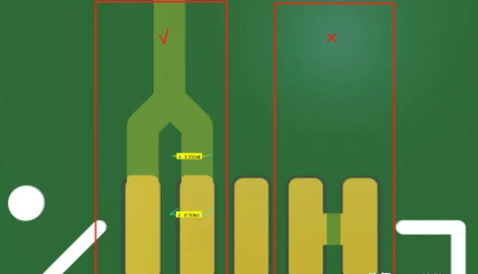
3.2 Routing and Signal Integrity
Common routing failures include:
- Insufficient clearance causing short circuits
- Acute angles leading to acid traps
- Overly long traces causing signal degradation
- Improper termination of high-speed signals
- Crosstalk between parallel traces
Effective routing practices:
- Follow manufacturer’s recommended routing guidelines
- Implement proper trace width for current carrying capacity
- Use appropriate spacing to prevent crosstalk
- Route critical signals first with shortest paths
- Avoid splitting reference planes under high-speed signals
3.3 Power Distribution Network (PDN) Design
PDN problems manifest as:
- Voltage drops causing logic errors
- Excessive noise on power rails
- Ground bounce issues
- EMI radiation from power loops
PDN design essentials:
- Use solid power and ground planes when possible
- Implement proper decoupling capacitor placement
- Consider power integrity analysis for complex designs
- Minimize loop areas in power delivery paths
- Use appropriate via stitching for plane connections
4. Design for Manufacturing (DFM) Considerations
Many PCB failures occur not because the design doesn’t work electrically, but because it cannot be reliably manufactured.
4.1 Fabrication Constraints
Ignoring fab house capabilities leads to:
- Higher costs due to special processing
- Increased scrap rates from marginal designs
- Delays while resolving manufacturability issues
Key fabrication considerations:
- Understand minimum trace/space capabilities
- Account for copper-to-edge clearance needs
- Follow hole size and aspect ratio guidelines
- Provide adequate solder mask clearance
- Include proper fiducials and tooling features
4.2 Assembly Considerations
Designs that are difficult to assemble result in:
- Poor solder joint quality
- Tombstoning of small components
- Shadowing during reflow
- Difficult inspection access
Assembly-friendly design practices:
- Follow component spacing guidelines
- Orient similar components in same direction
- Provide adequate solder paste relief
- Include test points for critical signals
- Consider automated optical inspection (AOI) requirements
5. Testing and Verification
Failure to properly verify the design before manufacturing often results in costly respins.
5.1 Design Rule Checking (DRC)
Comprehensive DRC should cover:
- Fabrication design rules
- Assembly design rules
- Electrical rule checks
- High-speed design rules
- Annular ring requirements
- Solder mask and silkscreen checks
5.2 Signal and Power Integrity Analysis
For complex designs, simulation helps identify:
- Signal quality issues
- Timing violations
- Power delivery problems
- EMI concerns
Analysis tools range from basic rule checkers to sophisticated 3D field solvers.
5.3 Prototyping and Testing
Physical verification methods:
- Bare board testing (opens/shorts)
- Assembly first article inspection
- Functional testing
- Environmental stress testing
- Long-term reliability testing
6. Documentation and Revision Control
Inadequate documentation causes:
- Manufacturing errors
- Assembly mistakes
- Difficult troubleshooting
- Costly re-engineering
Essential documentation includes:
- Complete fabrication drawings
- Assembly drawings with markings
- Bill of Materials (BOM) with approved alternates
- Test procedures and acceptance criteria
- Revision history and change tracking
Conclusion
Successful PCB design requires attention to numerous interrelated factors throughout the entire development process. From initial schematic capture to final manufacturing output, each decision carries implications for functionality, reliability, and cost. By understanding common failure modes and implementing proven best practices, engineers can significantly increase their chances of delivering successful PCB designs on the first attempt.
The most effective PCB designers adopt a holistic approach that balances electrical requirements with physical constraints, considers manufacturing realities during the design phase, and verifies all aspects of the design before release. In an era where electronic products face increasing performance demands while development cycles shrink, mastering these PCB design fundamentals becomes not just advantageous, but essential for competitive product development.
Remember that even experienced designers can overlook critical details—implementing thorough design reviews, checklists, and verification processes provides the safety net needed to catch potential issues before they become costly failures. By paying attention to the factors outlined in this article and continuously refining design practices based on lessons learned from each project, engineering teams can consistently produce high-quality PCB designs that meet all requirements for performance, reliability, and manufacturability.