Critical PCB Design Elements Impacting SMT Manufacturing
Abstract
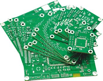
Surface Mount Technology (SMT) has revolutionized electronic manufacturing by enabling higher component density, improved performance, and reduced production costs compared to through-hole technology. However, the success of SMT manufacturing heavily depends on proper Printed Circuit Board (PCB) design. This paper examines the most critical PCB design elements that significantly influence SMT manufacturing outcomes, including pad design, component placement, thermal considerations, solder mask requirements, and panelization strategies. By understanding and optimizing these design elements, engineers can improve manufacturing yield, reliability, and reduce production costs.
1. Introduction
Surface Mount Technology has become the dominant assembly method in modern electronics, accounting for over 90% of all PCB assemblies today. The transition from through-hole to SMT components has enabled the miniaturization of electronic devices while improving their performance and reliability. However, this technological shift has introduced new design challenges that directly impact manufacturing outcomes.
PCB designers must consider numerous factors that affect the SMT assembly process, including solder joint formation, component placement accuracy, thermal management during reflow, and inspection requirements. Poor design choices can lead to manufacturing defects such as tombstoning, solder bridging, insufficient solder joints, or component misalignment—all of which reduce yield and increase production costs.
This paper systematically examines the key PCB design elements that influence SMT manufacturing, providing guidelines to optimize designs for manufacturability.
2. Pad Design and Layout
2.1 Pad Geometry and Dimensions
Pad design is perhaps the most critical element affecting SMT manufacturing quality. Proper pad dimensions must accommodate:
- Component terminal sizes
- Solder paste volume requirements
- Placement machine accuracy
- Thermal relief considerations
For standard two-terminal passive components (resistors, capacitors), the pad length should extend beyond the component terminal by 0.2-0.3mm to allow proper solder fillet formation. Pad width should match or slightly exceed (by 10-20%) the component terminal width.
2.2 Pad Spacing
Adequate spacing between pads prevents solder bridging:
- For fine-pitch components (<0.5mm pitch), reduce pad width to maintain 0.1-0.15mm spacing
- For standard pitch (≥0.5mm), maintain at least 0.2mm spacing between pads
2.3 Thermal Relief Pads
For components connected to large copper areas or ground planes:
- Use thermal relief connections (spokes) to prevent heat sinking during reflow
- Typical thermal relief designs use 4-6 spokes, 0.2-0.3mm wide
3. Component Placement Considerations
3.1 Orientation and Spacing
Uniform component orientation improves placement speed and accuracy:
- Orient all polarized components in the same direction when possible
- Maintain minimum spacing between components (typically 0.5mm for reflow, 1.0mm for wave solder)
3.2 Placement Accuracy Requirements
Consider pick-and-place machine capabilities:
- Standard machines: ±0.05mm accuracy
- High-precision machines: ±0.025mm accuracy
- Design placement tolerances accordingly
3.3 Heavy Component Placement
Large or heavy components (e.g., transformers, connectors):
- Place near the board center to prevent warping during reflow
- Provide additional mechanical support if needed
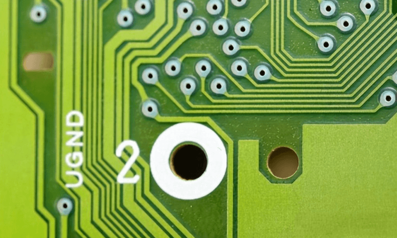
4. Solder Mask Design
4.1 Solder Mask Clearance
Proper solder mask clearance prevents solder wicking:
- Standard clearance: 0.05-0.1mm beyond pads
- For fine-pitch components: 0.025-0.05mm clearance
4.2 Solder Mask Between Pads
Critical for preventing solder bridging:
- Must cover all areas between pads for pitch <0.5mm
- Minimum solder mask web: 0.05mm for LPI (Liquid Photoimageable) masks
4.3 Solder Mask Material Selection
Choose based on application requirements:
- Standard: LPI solder mask (most common)
- High-density: Photo-Defined Dry Film (better resolution)
- High-reliability: Epoxy-based masks for harsh environments
5. Thermal Management in Design
5.1 Thermal Mass Distribution
Uneven thermal mass causes temperature variations during reflow:
- Balance copper distribution across layers
- Avoid large copper areas near small components
5.2 Thermal Pad Design
For components with thermal pads (QFN, DFN packages):
- Use 50-75% solder coverage on thermal pad
- Include adequate vias for heat dissipation (0.3mm diameter recommended)
5.3 Reflow Considerations
Design for proper heat transfer:
- Place heat-sensitive components away from high-mass areas
- Consider shadowing effects of tall components
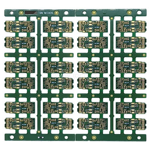
6. Panelization and Board Design
6.1 Panel Layout
Optimize panel utilization while considering:
- Fiducial marker placement
- Tooling hole requirements
- Breakaway tab design
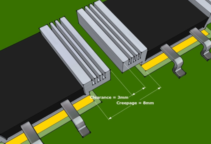
6.2 Board Edge Clearance
Maintain sufficient clearance for handling:
- Components: ≥3mm from board edge
- Traces: ≥0.5mm from board edge
6.3 Fiducial Markers
Essential for accurate component placement:
- Global fiducials: 3 markers, ≥5mm from board edges
- Local fiducials: For fine-pitch components, placed within 10mm of component
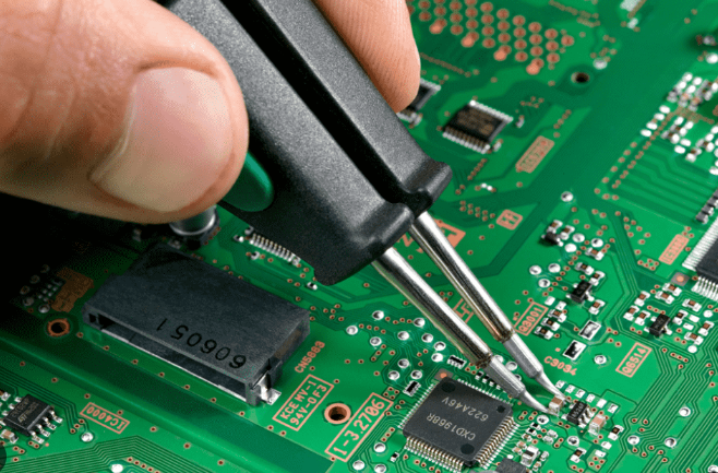
7. Design for Inspection and Testing
7.1 Automated Optical Inspection (AOI) Requirements
- Maintain adequate clearance around components for camera access
- Avoid placing tall components near small ones that need inspection
7.2 Test Point Accessibility
- Provide 0.8-1.0mm diameter test points for key signals
- Space test points ≥1.5mm apart for probe access
8. Emerging Design Considerations
8.1 Ultra-Fine Pitch Components
For components with <0.4mm pitch:
- Consider microvia technology
- Implement solder mask defined pads
- Use stepped solder masks
8.2 High-Density Interconnect (HDI) Designs
- Sequential lamination requirements
- Microvia placement constraints
- Laser drill alignment marks
9. Conclusion
PCB design elements profoundly influence the success of SMT manufacturing processes. By carefully considering pad designs, component placement strategies, thermal management requirements, and panelization approaches, designers can significantly improve manufacturing yields and product reliability. As component packages continue to shrink and board densities increase, these design considerations become even more critical.
Best practices in PCB design for SMT manufacturing include:
- Following IPC standards for pad geometries
- Maintaining consistent component orientation
- Implementing proper thermal relief designs
- Optimizing solder mask applications
- Designing for manufacturability from the initial layout phase
By addressing these critical design elements early in the development process, electronics manufacturers can reduce production costs, improve quality, and accelerate time-to-market for their products. Future advancements in SMT technology will require continued evolution of PCB design guidelines to address emerging challenges in miniaturization and high-speed performance