Cross Section PCB: An In-Depth Analysis of Design, Manufacturing, and Applications
1. Introduction to Cross Section PCB
Printed Circuit Boards (PCBs) are the backbone of modern electronics, providing mechanical support and electrical connectivity for electronic components. A cross-section PCB refers to the internal structure of a PCB that is revealed by cutting through the board and examining its layers. This technique is crucial for quality control, failure analysis, and design validation.
Understanding the cross-section of a PCB helps engineers and manufacturers ensure proper layer alignment, material integrity, and electrical performance. This article explores the key aspects of cross-section PCBs, including their structure, manufacturing processes, inspection techniques, and applications.
2. Structure of a PCB Cross-Section
A typical PCB consists of multiple layers, each serving a specific function. When examining a cross-section, the following layers are visible:
2.1 Substrate (Base Material)
- The core of the PCB is usually made of FR-4 (Flame Retardant-4), a glass-reinforced epoxy laminate.
- Other materials include polyimide (for flexible PCBs) and ceramic (for high-frequency applications).
2.2 Copper Layers
- Conductive traces carry electrical signals.
- PCBs can be single-sided, double-sided, or multilayer (4+ layers).
2.3 Prepreg (Pre-Impregnated Fiberglass)
- Acts as an adhesive between copper and core layers in multilayer PCBs.
- Provides insulation and structural stability.
2.4 Solder Mask
- A protective coating (usually green) that prevents short circuits and oxidation.
- Exposes only the necessary copper pads for soldering.
2.5 Silkscreen Layer
- Contains labels, component markings, and logos for assembly guidance.
2.6 Surface Finish
- Common finishes include HASL (Hot Air Solder Leveling), ENIG (Electroless Nickel Immersion Gold), and OSP (Organic Solderability Preservative).

3. Manufacturing Process of Multilayer PCBs
Creating a multilayer PCB involves several steps, and cross-section analysis ensures each layer meets specifications.
3.1 Layer Stackup Design
- Engineers define the number of layers, material types, and thicknesses.
- High-speed PCBs may use controlled impedance layers.
3.2 Inner Layer Fabrication
- Copper-clad laminates are etched to form circuit patterns.
- AOI (Automated Optical Inspection) checks for defects.
3.3 Lamination
- Inner layers are sandwiched with prepreg and outer copper foils.
- Heat and pressure bond the layers into a single board.
3.4 Drilling and Plating
- Laser or mechanical drills create vias (through-holes, blind/buried vias).
- Electroplating deposits copper inside vias for conductivity.
3.5 Outer Layer Patterning
- Photolithography transfers the circuit design onto the outer layers.
3.6 Solder Mask and Silkscreen Application
- UV curing hardens the solder mask.
- Silkscreen printing adds component labels.
3.7 Surface Finish and Testing
- Final plating (ENIG, HASL) ensures solderability.
- Electrical testing (Flying Probe, ICT) verifies connectivity.
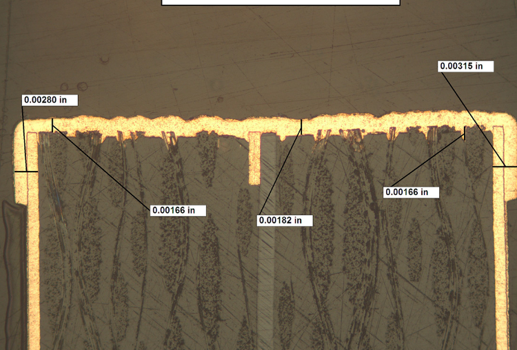
4. Importance of Cross-Section Analysis in PCB Inspection
Cross-sectioning is a destructive testing method that provides critical insights into PCB quality.
4.1 Defect Detection
- Delamination: Separation between layers due to poor lamination.
- Voiding: Air gaps in solder joints or plating.
- Microcracks: Fractures in copper traces or vias.
- Plating Thickness Variations: Uneven copper deposition.
4.2 Process Validation
- Ensures via integrity (no cracks or insufficient plating).
- Verifies layer alignment (misregistration causes shorts).
- Confirms solder mask thickness and coverage.
4.3 Failure Analysis
- Identifies root causes of PCB failures (thermal stress, mechanical damage).
- Helps improve manufacturing processes.
5. Techniques for PCB Cross-Sectioning
5.1 Sample Preparation
- Cutting: A diamond saw slices the PCB at the desired location.
- Encapsulation: The sample is embedded in epoxy for stability.
- Polishing: Grinding and polishing reveal a smooth cross-section.
5.2 Microscopic Examination
- Optical Microscopy: Low-magnification inspection.
- SEM (Scanning Electron Microscopy): High-resolution imaging.
- EDX (Energy-Dispersive X-ray Spectroscopy): Material composition analysis.
5.3 Non-Destructive Alternatives
- X-ray Imaging: Detects hidden defects without cutting.
- Acoustic Microscopy: Identifies delamination.
6. Applications of Cross-Section PCB Analysis
6.1 High-Reliability Electronics
- Aerospace, medical, and automotive PCBs require stringent quality checks.
- Ensures compliance with IPC-A-600 and MIL-STD-883 standards.
6.2 High-Density Interconnect (HDI) PCBs
- Verifies microvias and stacked vias in miniaturized designs.
6.3 Flexible and Rigid-Flex PCBs
- Checks adhesion between flexible and rigid sections.
6.4 Research and Development
- Helps optimize materials and manufacturing techniques.
7. Challenges in Cross-Section PCB Analysis
- Destructive Nature: The PCB is destroyed during inspection.
- Time-Consuming: Sample preparation requires precision.
- Interpretation Complexity: Requires skilled technicians.
8. Future Trends in PCB Cross-Section Technology
- Automated Cross-Sectioning: Robotics for faster sample prep.
- AI-Based Defect Detection: Machine learning for anomaly identification.
- 3D X-ray Tomography: Non-destructive 3D internal imaging.
9. Conclusion
Cross-section PCB analysis is a critical quality control tool that ensures the reliability and performance of modern electronics. By examining the internal structure of PCBs, manufacturers can detect defects, validate processes, and improve designs. As PCB technology advances, cross-sectioning techniques will continue to evolve, enabling higher precision and efficiency in electronics manufacturing.
For engineers and quality assurance teams, mastering cross-section analysis is essential for producing high-performance, defect-free PCBs in industries ranging from consumer electronics to aerospace.


