Crosstalk control of high-speed digital systems
Content: Crosstalk is perhaps the most difficult to understand and predict in high frequency circuits, however, it can be controlled and even eliminated.
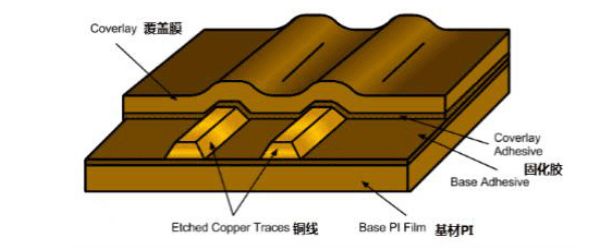
As switching speeds increase, modern digital systems encounter a series of problems, such as signal reflection, delay fading, crosstalk, and electromagnetic compatibility failure. When the switching time of integrated circuits drops to 5 nanoseconds or 4 nanoseconds or lower, the inherent characteristics of the printed circuit board itself start to show up. Unfortunately, these properties are harmful and should be avoided during the design process.
Crosstalk is perhaps the most difficult to understand and predict among high frequency circuits, however, it can be controlled and even eliminated.
1.What causes crosstalk?
When a signal travels along the wiring of a printed circuit board, its electromagnetic waves also propagate along the wiring, from one end of the integrated circuit chip to the other end of the line. During propagation, electromagnetic waves cause transient voltages and currents due to electromagnetic induction.
Electromagnetic waves include electric and magnetic fields that change over time. In printed circuit boards, in fact, the electromagnetic field is not limited to various wirings, and a considerable part of the electromagnetic field energy exists outside the wiring. So, if there are other lines nearby, when a signal travels along one wire, its electric and magnetic fields will affect other lines. According to Maxwell’s equations, time-varying electric and magnetic fields will cause voltages and currents in adjacent conductors. Therefore, the electromagnetic fields accompanying the signal propagation process will cause adjacent lines to generate signals, thus leading to crosstalk.
In printed circuit boards, lines that cause crosstalk are often called “intruders.” Lines affected by crosstalk are often called “victims.” The crosstalk signals in any “victim” can be divided into forward crosstalk signals and backward crosstalk signals, which are caused in part by capacitive and inductive coupling. The mathematical description of crosstalk signals is very complex, but, like a speedboat on a lake, certain quantitative characteristics of forward and backward crosstalk signals can still be understood.
A high-speed boat has two effects on the water. First, the speedboat stirs up waves on the bow, and the arc-shaped ripples seem to move forward with the speedboat; secondly, when the speedboat travels for a period of time, it will leave long water trails behind it.
This is very similar to the reaction of the “victim” when the signal passes through the “intruder”. There are two kinds of crosstalk signals in the “victim”: the forward signal that is before the intruder signal, like water and ripples on the bow of a boat; the backward signal that lags behind the intruder signal, like the water traces that remain in the lake after the boat has moved away. .
2.Capacitive characteristics of forward crosstalk
Forward crosstalk manifests itself in two interrelated properties: capacitive and perceptual. When the “intrusion” signal advances, a voltage signal in the same phase as the “intrusion” signal is generated in the “victim”. This signal has the same speed as the “intrusion” signal, but is always before the “intrusion” signal. This means that the crosstalk signal does not propagate ahead of time, but travels at the same speed as the “intrusion” signal and couples in more energy.
Since the crosstalk signal is caused by changes in the “intrusion” signal, the forward crosstalk pulse is not unipolar but has both positive and negative polarities. The pulse duration is equal to the switching time of the “intrusion” signal.
The coupling capacitance between the wires determines the amplitude of the forward crosstalk pulse, and the coupling capacitance is determined by many factors, such as the material of the printed circuit board, the geometric size, the location of the line crossing, etc. The amplitude is proportional to the distance between parallel lines: the longer the distance, the larger the crosstalk pulse. However, there is an upper limit to the crosstalk pulse amplitude, as the “intruder” signal gradually loses energy and the “victim” in turn couples back to the “intruder”. Inductive Characteristics of Forward Crosstalk
When an “intrusive” signal propagates, its time-varying magnetic field also produces crosstalk:
forward crosstalk with inductive properties. But perceptual crosstalk and capacitive crosstalk are obviously different:
the polarity of forward perceptual crosstalk is opposite to the polarity of forward capacitive crosstalk. This is because in the forward direction, the capacitive part and the perceptual part of the crosstalk are competing and canceling each other out. In fact, when forward capacitive and perceptual crosstalk are equal, there is no forward crosstalk.
In many devices, forward crosstalk is quite small, while backward crosstalk becomes a major problem, especially on long strip circuit boards, because capacitive coupling is enhanced. However, without simulation, it is actually impossible to know to what extent the perceptual and capacitive crosstalk cancel out.
If you measure forward crosstalk, you can tell whether your traces are capacitively or inductively coupled based on their polarity. If the crosstalk polarity is the same as the “intrusion” signal, capacitive coupling will dominate; otherwise, inductive coupling will dominate. In printed circuit boards, it is usually the inductive coupling that is stronger.
The physics of backward crosstalk are the same as forward crosstalk: the time-varying electric and magnetic fields of the “invading” signal cause inductive and capacitive signals in the “victim”. But there are differences between the two.

The biggest difference is the duration of the backward crosstalk signal.
Because the forward crosstalk and the “intrusion” signal propagate in the same direction and at the same speed, the duration of the forward crosstalk is the same as the “intrusion” signal. However, backward crosstalk and the “intrusion” signal travel in the opposite direction, it lags behind the “intrusion” signal and causes a long train of pulses.
Unlike forward crosstalk, the amplitude of the backward crosstalk pulse is independent of line length, and its pulse duration is twice the delay time of the “intrusion” signal. Why? Suppose you look at backward crosstalk from the signal’s origin point. As the “invading” signal moves away from the origin point, it is still generating backward pulses until another delayed signal appears. Thus, the entire duration of the backward crosstalk pulse is twice the delay time of the “intrusion” signal.
3.Reflection of backward crosstalk
You may not care about crosstalk interference between the driver chip and the receiver chip. However, why should you care about backward pulses? Because the driver chip generally has a low-impedance output, it reflects more crosstalk signals than it absorbs. When the backward crosstalk signal reaches the “victim”‘s driver chip, it is reflected back to the receiving chip. Because the output resistance of the driver chip is generally lower than the wire itself, it often causes reflection of the crosstalk signal.
Unlike the forward crosstalk signal, which has both inductive and capacitive characteristics, the backward crosstalk signal has only one polarity, so the backward crosstalk signal cannot cancel itself. The polarity of the backward crosstalk signal and the crosstalk signal after its reflection is the same as the “intrusion” signal, and its amplitude is the sum of the two parts.
Remember, when you detect a backward crosstalk pulse at the receiving end of the “victim”, the crosstalk signal has already been reflected by the “victim” driver chip. You can observe that the polarity of the backward crosstalk signal is opposite to that of the “intrusion” signal.
In digital design, you often care about some quantitative indicators, such as: regardless of how and when crosstalk is generated, forward or backward, its maximum noise margin is 150mV. So, is there a simple way to accurately measure noise? The simple answer is “no”, because the electromagnetic field effect is too complicated and involves a series of equations, the topology of the circuit board, the analog characteristics of the chip, etc.
4.Crosstalk elimination
From a practical point of view, the most important issue is how to remove crosstalk. What should you do when crosstalk affects circuit characteristics?
There are two strategies you can adopt. One approach is to change one or more geometric parameters that affect coupling, such as trace length, distance between traces, and layering locations on the circuit board. Another method is to use terminals to change single lines into multi-channel coupled lines. Properly designed, multi-line terminals can eliminate most crosstalk.
5.Line length
Many designers believe that shortening line length is the key to reducing crosstalk. In fact, almost all circuit design software provides the function of controlling the length of the maximum parallel lines. Unfortunately, it is difficult to reduce crosstalk by simply changing the geometric values.
Because forward crosstalk is affected by coupling length, there is little reduction in crosstalk when you shorten the length of a line that is not coupled. Furthermore, if the coupling length exceeds the falling or rising delay of the driver chip, the linear relationship between coupling length and forward crosstalk will reach a saturation value. At this time, shortening the already long coupling line will have little effect on reducing crosstalk.
A reasonable approach is to extend the distance between coupling lines. In almost all cases, split coupling lines can greatly reduce crosstalk interference. Practice has proven that the amplitude of backward crosstalk is roughly inversely proportional to the square of the distance between coupled lines, that is: if you double this distance, the crosstalk is reduced by three-quarters. This effect is even more pronounced when backward crosstalk dominates.
6.Isolation difficulty
It is not easy to increase the distance between coupling lines. If your wiring is very dense, you have to put a lot of effort into reducing the wiring density. If you’re worried about crosstalk, you can add one or two isolation layers. If you have to extend the distance between lines or networks, you’d better have software that makes it easy to do so. Line width and thickness also affect crosstalk interference, but their impact is much smaller than the distance factor of the line. Therefore, these two parameters are generally rarely adjusted.
Because the insulating material of the circuit board has a dielectric constant, it will also produce coupling capacitance between lines, so lowering the dielectric constant can also reduce crosstalk interference. This effect is not very obvious, especially in microstrip circuits where part of the dielectric is already air. What’s more, changing the dielectric constant is not that easy, especially in expensive equipment. A workaround is to use more expensive materials instead of FR-4.
The thickness of the dielectric affects crosstalk interference over a large length. Generally, placing the wiring layer close to the power layer (Vcc or ground) can reduce crosstalk interference. The precise value of the improvement effect needs to be determined through simulation.
7.Stratification factors
Some PCB designers still don’t pay attention to layering methods, which is a major mistake in high-speed circuit design. Lamination not only affects the performance of transmission lines, such as impedance, delay, and coupling, but the circuit operation is prone to abnormalities or even changes. For example, reducing crosstalk interference by reducing the dielectric thickness by 5 mil is not possible, although it can be achieved in terms of cost and process.
Another easily overlooked factor is layer selection. Many times, forward crosstalk is the dominant crosstalk interference in microstrip circuits. However, if designed properly, the routing layer is placed between the two power planes, so that capacitive and inductive coupling are well balanced, and backward crosstalk with lower amplitude becomes the dominant factor. Therefore, you must pay attention to which crosstalk interference is dominant during simulation.
The positional relationship between wiring and chips also affects crosstalk.
Because the backward crosstalk reaches the receiving chip and is reflected to the driver chip, the location and performance of the driver chip are very important. Because of the complexity of topology, reflections and other factors, it is difficult to explain who is primarily responsible for crosstalk. If there are multiple topologies to choose from, it is best to run simulations to determine which structure has the least impact on crosstalk.
One non-geometric factor that may reduce crosstalk is the specification of the driver chip itself. The general principle is to choose a driver chip with a long switching time to reduce crosstalk interference (the same goes for solving many other problems caused by high speed). Even if crosstalk is not strictly proportional to switching time, reducing switching time can still have a significant impact.
Many times, you can’t choose the driver chip technology, you can only change the geometric parameters to achieve the goal. Reduce crosstalk through terminals
It is well known that if an independent, uncoupled transmission line is terminated with matching impedance, it will not produce reflections. Now consider a series of coupled transmission lines, for example, three transmission lines that have crosstalk with each other, or a pair of coupled transmission lines.
If you use circuit analysis software, you can derive a pair of matrices representing the capacitance and inductance of the transmission line itself and each other. For example,
three transmission lines might have the following C and L matrices:
In these matrices, the diagonal elements are the values of the transmission lines themselves, and the off-diagonal elements are the values of the transmission lines relative to each other. (Note that they are expressed in pF and nH per unit length).
These values can be determined with a sophisticated electromagnetic field tester.
It can be seen that each set of transmission lines also has a characteristic impedance matrix. In this Z0 matrix, the diagonal elements represent the impedance value of the transmission line to the ground line, and the off-diagonal elements are the transmission line coupling values.
For a group of transmission lines, similar to a single transmission line, if the terminal is an impedance array matched to Z0, its matrix is almost the same. The required impedance does not have to be the value in Z0, as long as the resulting impedance network matches Z0. The impedance matrix includes not only the impedance of the transmission line to the ground, but also the impedance between the transmission lines.
Such an impedance array has good properties. First, it prevents reflections of crosstalk in uncoupled lines. More importantly, it can eliminate crosstalk that has already formed.
8.Lethal weapons
Unfortunately, such a termination is expensive and not ideal because the coupling impedance between some transmission lines is too small, causing large currents to flow into the driver chip. The impedance between the transmission line and ground also cannot be so great that it cannot drive the chip. If these problems exist and you plan to use this type of terminal, try adding a few AC coupling capacitors.
Although there are some difficulties in implementation, impedance array termination is still a lethal weapon against signal reflections and crosstalk, especially in harsh situations. It may or may not work in other circumstances, but it’s still a recommended approach.