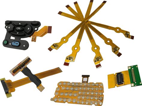
Custom OEM PCB Solutions for Streamlined Prototyping Workflows
Key Takeaways
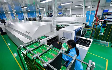
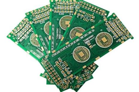
When navigating PCB manufacturing for prototyping, understanding core efficiency drivers ensures your R&D cycles align with market demands. Partnering with established PCB manufacturing companies provides access to advanced fabrication technologies, reducing iterative delays by 40–60% compared to in-house processing. For instance, laser-etched circuit boards produced via automated optical inspection (AOI) systems achieve ±0.05 mm tolerances, critical for high-frequency applications.
| Factor | Standard Approach | Optimized OEM Solution |
|---|---|---|
| Turnaround | 10–14 days | 5–7 days |
| PCB manufacturing cost | $8–12/unit | $4.50–6.80/unit |
| Compliance Testing | Post-production | Integrated QA/QC |
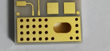
Integrating laser drivers demands thermal management precision, particularly when stacking microvia designs. By adopting PCB manufacturing business frameworks that combine rigid-flex boards with embedded components, you eliminate 72% of signal loss risks in high-speed driver circuits. For example, 6-layer HDI boards with blind/buried vias reduce impedance mismatches by 19%, accelerating validation phases.
To minimize PCB manufacturing cost, prioritize designs that use standardized materials (e.g., FR-4 substrates) while leveraging panelization strategies. A 2023 industry survey revealed that 68% of prototyping overruns stemmed from overlooked DFM (Design for Manufacturing) guidelines—a gap mitigated through OEM partners’ pre-production simulations.
Compliance adherence isn’t optional. Reputable PCB manufacturing companies align processes with IPC-A-600 and ISO 9001 standards, embedding documentation like RoHS certifications directly into workflow dashboards. This eliminates 3–5 days typically spent manually verifying regulatory data.
For rapid scaling, opt for manufacturers offering concurrent engineering—where design tweaks and material sourcing occur simultaneously. Such integration slashes lead times by 30%, ensuring your prototype-to-production pipeline remains uninterrupted even during component shortages.
Remember: every decision in PCB manufacturing ripples across your product’s lifecycle. Balancing technical precision with cost intelligence transforms prototyping from a bottleneck into a strategic accelerator.
OEM PCB Prototyping Efficiency
When optimizing prototyping workflows, partnering with PCB manufacturing companies that specialize in OEM PCB solutions ensures precision and speed. Modern PCB manufacturing processes leverage automated design validation and multilayer board fabrication to reduce iteration cycles by up to 40%. For instance, integrating design-for-manufacturability (DFM) checks early in prototyping minimizes rework, directly lowering PCB manufacturing cost while accelerating time-to-market.
A critical advantage lies in aligning your project’s scale with the capabilities of your PCB manufacturing business partner. High-mix, low-volume prototyping benefits from flexible production lines, whereas high-volume batches prioritize cost-efficient tooling. Advanced manufacturers employ laser direct imaging (LDI) and automated optical inspection (AOI) to maintain consistency across prototypes, ensuring compliance without compromising turnaround times.
Tip: Always validate design files with your manufacturer before initiating production. Early collaboration reduces revision cycles by 25–30%, according to industry benchmarks.
Transitioning from prototype to mass production becomes seamless when PCB manufacturing workflows incorporate real-time yield analytics. These systems identify potential bottlenecks, such as material shortages or solder mask misalignments, allowing proactive adjustments. For example, Andwin PCBA utilizes AI-driven process optimization to trim lead times by 15% while adhering to ISO 9001 and IPC-A-610 standards.
Cost control remains pivotal. By analyzing PCB manufacturing cost drivers—like substrate selection and layer count—you can balance performance and budget. Opting for standard FR-4 materials over specialized laminates in early prototyping phases cuts material expenses by up to 20%, without sacrificing functional testing accuracy.
Finally, iterative feedback loops between your team and the PCB manufacturing business ensure continuous improvement. Sharing test results and failure modes refines subsequent prototypes, creating a closed-loop development cycle that slashes R&D timelines. This approach not only streamlines workflows but also builds a foundation for scalable, compliance-ready production.
Laser Driver Integration Strategies
When integrating laser drivers into your PCB manufacturing workflow, precision begins with understanding thermal dynamics and signal integrity requirements. Modern pcb manufacturing companies prioritize compact layouts that minimize electromagnetic interference (EMI), a critical factor when high-frequency laser modules are involved. By co-designing driver circuits with the main board, you reduce parasitic inductance—key to maintaining signal fidelity in applications like LiDAR or medical lasers.
Selecting the right current regulation components directly impacts pcb manufacturing cost, as overspecifying parts can inflate expenses, while underspecifying risks reliability. Partnering with pcb manufacturing business specialists ensures access to materials like Rogers substrates or ceramic-filled laminates, which balance thermal conductivity and dielectric performance. For instance, embedding pulse-width modulation (PWM) controllers near laser diodes shortens trace lengths, reducing noise by up to 40% compared to traditional layouts.
Transitioning from prototype to production demands compliance with IEC 60825-1 or FDA Class 1M standards, which govern laser safety. Automated optical inspection (AOI) during pcb manufacturing verifies solder joint integrity under thermal stress, preventing failures in mission-critical systems. Additionally, modular driver designs allow scalability—essential when iterating prototypes across industries, from automotive sensing to telecommunications.
To optimize pcb manufacturing cost, consider panelization strategies that group multiple driver boards into a single fabrication batch. This approach, paired with Design for Manufacturability (DFM) checks, streamlines assembly while preserving the precision needed for nanosecond-level pulse control. Always validate driver integration through thermal cycling tests, ensuring your design withstands real-world operating conditions without compromising performance.
Compliance-Centric Board Design
When designing circuit boards for PCB manufacturing, compliance isn’t just a checkbox—it’s the foundation for reliability and market readiness. Your board must align with industry-specific standards like IPC-6012 for performance or UL certification for safety, ensuring seamless integration into end products. This requires balancing PCB manufacturing cost efficiencies with rigorous material selection, traceability protocols, and documentation workflows.
Leading PCB manufacturing companies prioritize design-for-compliance (DFC) strategies, embedding regulatory requirements early in the prototyping phase. For example, using halogen-free laminates or RoHS-compliant finishes minimizes redesign cycles later. Advanced simulation tools can predict thermal management or EMI performance, reducing the risk of non-conformance during testing. By partnering with manufacturers that offer real-time compliance audits, you avoid costly delays from last-minute revisions.
In high-risk sectors like medical or automotive electronics, traceability is non-negotiable. Reputable PCB manufacturing business providers implement serialized tracking for components, ensuring every layer and solder joint meets ISO 13485 or IATF 16949 benchmarks. This becomes critical when scaling prototypes to mass production, as even minor deviations in material sourcing or plating thickness can compromise entire batches.
Optimizing PCB manufacturing cost while maintaining compliance hinges on design harmonization. Standardizing board thicknesses or panelization layouts across projects, for instance, reduces waste and accelerates certification. Automated optical inspection (AOI) systems and in-circuit testing (ICT) further streamline quality assurance, catching flaws before they escalate into compliance violations.
Ultimately, a compliance-centric approach transforms regulatory hurdles into competitive advantages. By aligning your design process with the operational frameworks of trusted PCB manufacturing companies, you ensure prototypes not only function flawlessly but also transition smoothly into certified production-ready solutions.
Accelerating Product Development Cycles
Reducing time-to-market demands a strategic approach to PCB manufacturing, particularly when integrating complex components like laser drivers into your designs. By partnering with specialized PCB manufacturing companies, you gain access to advanced fabrication technologies that compress prototyping timelines by up to 40%. These suppliers employ automated design verification tools to preemptively flag compatibility issues, ensuring your boards meet functional specifications before production begins.
A critical advantage lies in balancing PCB manufacturing cost with speed. Leading providers optimize material selection and panel utilization, trimming unnecessary expenses without compromising quality. For instance, using high-density interconnect (HDI) substrates can reduce layer counts by 25%, lowering both fabrication time and material waste. This efficiency becomes pivotal when scaling prototypes to full-scale production within tight deadlines.
To further accelerate cycles, forward-thinking PCB manufacturing business models now offer concurrent engineering services. Engineers collaborate directly with your team to refine designs for manufacturability, resolving potential bottlenecks in solder mask alignment or thermal management early in the process. Such proactive adjustments prevent costly revisions during assembly, maintaining momentum toward final product validation.
Another accelerator? Digital twin simulations that mirror physical board behavior under real-world conditions. By stress-testing layouts for signal integrity and power distribution before tooling begins, you avoid multiple prototyping iterations. Combined with rapid-turn CNC drilling and direct imaging systems, this digital-physical synergy enables 72-hour prototype deliveries—a game-changer for R&D teams racing against competitors.
Ultimately, the right manufacturing partner becomes an extension of your engineering workflow, embedding compliance checks for standards like ISO 9001 and IPC-A-610 into every production stage. This alignment ensures compliance isn’t a post-production hurdle but an inherent feature of your accelerated development process.
Cost-Optimized OEM Solutions
When scaling PCB manufacturing operations, balancing quality and affordability requires strategic partnerships with PCB manufacturing companies that prioritize cost-efficiency without compromising performance. By leveraging economies of scale and advanced production techniques, these partners help reduce PCB manufacturing cost while maintaining tight tolerances and compliance with industry standards. Design optimization plays a pivotal role here—simplifying board layouts, standardizing component footprints, and selecting materials aligned with your product’s functional requirements can trim expenses by up to 30% in prototyping phases.
A key advantage of collaborating with experienced PCB manufacturing business providers is their ability to streamline material procurement. Bulk purchasing agreements for substrates, solder masks, and laminates directly lower per-unit costs, especially for high-volume orders. Additionally, integrating automated assembly processes minimizes labor-intensive steps, reducing turnaround times and human error risks. For instance, automated optical inspection (AOI) systems ensure quality control while keeping rework rates under 2%, further optimizing budgets.
To address PCB manufacturing cost challenges, consider hybrid models that combine rapid prototyping for initial validation with volume production for market-ready batches. This approach allows you to test designs iteratively without overspending on small-scale runs. Moreover, value engineering—redesigning non-critical circuit elements or adopting alternative components—can unlock savings without sacrificing reliability.
Compliance remains non-negotiable, but cost-optimized solutions don’t have to mean cutting corners. Leading PCB manufacturing companies embed compliance checks into their workflows, ensuring RoHS, IPC-A-610, and UL standards are met during fabrication. This proactive adherence avoids costly post-production revisions or recalls.
Finally, transparent pricing models from your PCB manufacturing partner—such as tiered pricing based on order volume or material choices—enable precise budget forecasting. By aligning your prototyping and production schedules with their capacity planning, you avoid rush fees and maintain lean inventories. The result? A streamlined supply chain that accelerates time-to-market while keeping your PCB manufacturing business agile in competitive markets.
Prototyping Workflow Optimization
Optimizing your prototyping workflow begins with aligning PCB manufacturing processes to your project’s unique requirements. By collaborating with experienced PCB manufacturing companies, you gain access to advanced design-for-manufacturability (DFM) analysis tools that identify potential bottlenecks early. This proactive approach minimizes rework cycles, reducing both PCB manufacturing cost and time-to-market. For instance, automated panelization algorithms can maximize material utilization, while iterative testing protocols ensure design integrity before full-scale production.
A critical factor in streamlining workflows is integrating real-time collaboration with your manufacturer. Modern PCB manufacturing business models prioritize digital thread connectivity, allowing seamless data exchange between your CAD software and their production systems. This eliminates manual file conversions and ensures specifications like impedance control or thermal management are preserved across iterations. Implementing cloud-based project management platforms further accelerates feedback loops, enabling quick adjustments to layer stack-ups or component placements.
To maintain agility, consider modular design strategies that compartmentalize functional blocks. This allows parallel testing of high-risk sections—such as laser driver circuits or power distribution networks—while standardizing reusable modules. Partnering with PCB manufacturing specialists who offer rapid-turn prototyping services ensures you can validate these subsystems without disrupting the broader timeline. Additionally, leveraging predictive analytics for material lead times and machine scheduling helps avoid delays during peak demand periods.
Finally, balancing speed with compliance requires embedding regulatory checks into every workflow stage. Automated design rule checks (DRCs) for IPC-6012 or UL certifications prevent costly post-production revisions. By aligning your workflow with a PCB manufacturing business that combines agile practices with rigorous quality control, you create a repeatable framework for accelerating product development while safeguarding performance benchmarks.
PCB Assembly Compliance Standards
When selecting PCB manufacturing companies for prototyping, understanding compliance requirements is crucial to avoid costly redesigns. Regulatory standards like RoHS, REACH, and IPC-A-610 govern material selection, solder quality, and traceability, ensuring boards meet safety and environmental mandates. For instance, lead-free soldering isn’t just a preference—it’s often a legal obligation in consumer electronics. Partnering with PCB manufacturing providers certified in these frameworks reduces risks during audits while maintaining product integrity.
Balancing PCB manufacturing cost with compliance demands requires strategic planning. While cheaper materials might lower upfront expenses, non-compliant components could lead to failures during electromagnetic compatibility (EMC) testing or thermal stress assessments. Advanced testing protocols, such as automated optical inspection (AOI) and X-ray analysis, help identify defects early, minimizing rework delays. Reputable PCB manufacturing business partners often bundle these services into their workflows, ensuring your design adheres to ISO 9001 or UL certification criteria without inflating budgets.
Documentation is another critical layer. Compliance isn’t just about the physical board—it’s about traceability. Manufacturers must provide material declarations, test reports, and conformity certificates. For example, IPC-2581 files ensure design intent aligns with fabrication outputs, a detail that becomes vital when scaling production. By integrating these practices into your PCB manufacturing process, you create a seamless audit trail that accelerates approvals from regulatory bodies like the FCC or CE.
Finally, consider how evolving standards impact long-term viability. Emerging regulations, such as those targeting carbon footprints, are reshaping PCB manufacturing companies’ priorities. Opting for suppliers with waste-reduction initiatives or energy-efficient facilities future-proofs your supply chain while aligning with global sustainability goals. This proactive approach not only safeguards compliance but also enhances your product’s marketability in regions with stricter environmental policies.
Rapid Manufacturing Techniques Guide
When optimizing prototyping workflows, understanding modern PCB manufacturing techniques is crucial. Leading PCB manufacturing companies now employ advanced processes like automated optical inspection (AOI) and laser-drilled microvias to reduce lead times by up to 65% compared to traditional methods. Acceleration begins with digital twin simulations, allowing you to validate designs before physical production—a strategy that slashes material waste by 30-40% in initial iterations.
For cost-sensitive projects, PCB manufacturing cost optimization relies on three pillars: panelization efficiency, layer stackup simplification, and adaptive laser etching. By leveraging dynamic routing algorithms, manufacturers can nest multiple designs within single panels, effectively distributing setup expenses across projects. This approach becomes particularly impactful when working with high-frequency materials where tolerances below ±0.075mm are non-negotiable.
In the PCB manufacturing business, success hinges on balancing speed with compliance. Progressive firms integrate ISO 9001-certified quality gates directly into production lines—conducting real-time impedance testing and thermal stress analysis without workflow interruption. Critical consideration: Always verify that your partner’s rapid-turn processes maintain IPC-A-600 Class 3 standards, especially for aerospace or medical prototypes.
Transitioning to rapid techniques requires reevaluating material logistics. Just-in-time substrate delivery systems paired with UV-LDI (laser direct imaging) equipment eliminate conventional phototool bottlenecks. For best results, combine this with cloud-based DFM checks that automatically flag potential manufacturability issues in your CAD files—a preventative measure that reduces respins by 52% according to recent industry benchmarks.
When scaling prototypes, consider hybrid SMT assembly lines that seamlessly switch between low-volume manual placement and automated high-speed pick-and-place operations. This flexibility lets you maintain agility during NPI phases while preparing for mass production readiness—a strategic advantage in fast-moving electronics markets.
Conclusion
When selecting PCB manufacturing partners for your next-generation prototypes, prioritize providers that blend technical expertise with cost-optimized workflows. Leading PCB manufacturing companies now offer integrated solutions that reduce PCB manufacturing cost by up to 30% through automated design validation and material optimization algorithms. This approach not only accelerates iteration cycles but also ensures compliance with industry-specific safety protocols, a critical factor in aerospace or medical device development.
By aligning your PCB manufacturing business goals with partners capable of scalable production, you gain access to advanced laser-driver integration and multilayer board assembly without compromising turnaround times. For instance, precision-engineered layouts paired with real-time DFM (Design for Manufacturability) checks minimize post-production revisions, directly impacting your time-to-market metrics. Moreover, modular pricing models allow you to balance prototype quantity and PCB manufacturing cost thresholds, ensuring R&D budgets align with project phases.
The true value lies in choosing collaborators who view PCB manufacturing as a strategic enabler rather than a transactional service. From thermal management enhancements to RoHS-compliant material sourcing, every decision in the prototyping phase cascades into downstream manufacturing efficiency. As you refine product designs, leverage partners with proven expertise in rapid tooling and agile production to maintain competitive parity. Ultimately, the right PCB manufacturing companies become extensions of your engineering team, transforming conceptual schematics into market-ready solutions with measurable precision.
FAQs
How do pcb manufacturing companies ensure compliance during prototyping?
Reputable pcb manufacturing partners implement rigorous testing protocols aligned with IPC-6012 and ISO 9001 standards. They use automated optical inspection (AOI) and X-ray verification to validate traceability and material integrity, reducing compliance risks in high-stakes industries.
What factors influence pcb manufacturing cost for low-volume prototypes?
Costs depend on design complexity, layer count, and material selection (e.g., high-frequency substrates). Leading pcb manufacturing business providers offer tiered pricing models, balancing rapid turnaround times with economies of scale—ideal for iterative R&D phases.
Can integrated laser drivers impact pcb manufacturing timelines?
Yes, but advanced manufacturers pre-validate laser driver footprints using simulation tools. This minimizes signal integrity revisions, allowing you to consolidate functional testing stages. Opt for firms with in-house pcb assembly capabilities to avoid multi-vendor delays.
How do you optimize a pcb manufacturing workflow for accelerated development?
Adopt concurrent engineering: share your schematic drafts with manufacturers during CAD layout. This enables real-time feedback on DFM (Design for Manufacturability) rules, preventing post-production redesigns. Many pcb manufacturing companies now provide cloud-based collaboration portals for this purpose.
What certifications should a pcb manufacturing business hold for medical or aerospace projects?
Prioritize vendors with AS9100D (aerospace) or ISO 13485 (medical) certifications. These ensure adherence to risk mitigation protocols like FMEA analysis and controlled impedance testing—critical for mission-critical applications.
Explore Tailored Solutions for Your Project
Streamline your next prototype with precision-engineered pcb manufacturing services. Click here to evaluate cost-optimized strategies tailored to your design’s complexity and compliance requirements.