Custom pcb board design
Benefits Of Custom PCB Board Design For Startups
Custom PCB board design offers a multitude of benefits for startups, providing them with a competitive edge in the rapidly evolving technological landscape. As startups strive to innovate and differentiate themselves, the ability to tailor printed circuit boards (PCBs) to specific needs becomes increasingly valuable.
One of the primary advantages of custom PCB design is the enhanced flexibility it offers.
Unlike off-the-shelf solutions, custom PCBs can be designed to meet the exact specifications required by a startup’s unique product or application. This level of customization ensures that the PCB fits perfectly within the product’s form factor, optimizing space and improving overall functionality.
Moreover, custom PCB design allows startups to integrate multiple functions onto a single board, reducing the need for additional components and thereby minimizing costs.
This integration not only streamlines the manufacturing process but also enhances the reliability of the final product by reducing potential points of failure. As a result, startups can deliver high-quality products to market more efficiently, which is crucial in maintaining a competitive advantage.
In addition to cost efficiency, custom PCB design contributes to improved performance.
By tailoring the board to specific requirements, startups can optimize the electrical performance of their products. This optimization can lead to faster processing speeds, lower power consumption, and enhanced signal integrity, all of which are critical factors in the development of cutting-edge technology. Furthermore, custom PCBs can be designed to accommodate future upgrades or modifications, providing startups with the flexibility to adapt to changing market demands without the need for a complete redesign.
Another significant benefit of custom PCB design is the potential for innovation.
Startups are often at the forefront of technological advancements, and having the ability to design PCBs from scratch allows them to experiment with new ideas and concepts. This freedom fosters creativity and can lead to the development of groundbreaking products that set a startup apart from its competitors. Additionally, custom PCBs can be designed to incorporate the latest technologies and components, ensuring that startups remain at the cutting edge of their respective industries.
Furthermore, custom PCB design can enhance a startup’s brand identity.
By creating unique and innovative products, startups can establish themselves as leaders in their field, attracting attention from investors, partners, and customers alike. A well-designed custom PCB can serve as a testament to a startup’s commitment to quality and innovation, reinforcing its reputation and credibility in the market.
Finally, custom PCB design can facilitate compliance with industry standards and regulations.
Startups often operate in highly regulated environments, and ensuring that their products meet all necessary requirements is essential for success. Custom PCBs can be designed with these standards in mind, reducing the risk of non-compliance and potential legal issues. This proactive approach not only safeguards the startup’s operations but also instills confidence in stakeholders.
In conclusion, custom PCB board design offers numerous benefits for startups, from cost efficiency and improved performance to innovation and compliance.
By leveraging these advantages, startups can position themselves for success in a competitive market, delivering high-quality, cutting-edge products that meet the needs of their customers and drive their growth. As technology continues to advance, the importance of custom PCB design will only increase, making it an indispensable tool for startups aiming to thrive in the digital age.
Key Considerations In Custom PCB Board Design
When embarking on the journey of custom PCB board design, several key considerations must be meticulously evaluated to ensure the successful development of a functional and efficient printed circuit board. The process begins with a clear understanding of the project requirements, which serves as the foundation for all subsequent design decisions. This involves defining the board’s purpose, the environment in which it will operate, and the specific electrical and mechanical constraints it must adhere to. By establishing these parameters early on, designers can make informed choices that align with the overall objectives of the project.
Transitioning from the initial planning phase, the next critical step involves selecting the appropriate materials and components.
The choice of substrate material, such as FR-4, polyimide, or metal-core, can significantly impact the board’s performance, particularly in terms of thermal management and signal integrity. Additionally, the selection of components must consider factors such as size, power consumption, and compatibility with the board’s layout. It is essential to strike a balance between performance and cost, ensuring that the chosen components meet the design specifications without exceeding budgetary constraints.
As the design progresses, attention must be paid to the layout and routing of the PCB.
This stage is crucial, as it directly affects the board’s electrical performance and manufacturability. Designers must carefully plan the placement of components to minimize signal interference and optimize the flow of electrical currents. Furthermore, routing strategies should be employed to reduce the risk of crosstalk and electromagnetic interference, which can degrade the board’s functionality. Utilizing advanced design software can aid in visualizing and simulating the layout, allowing for adjustments to be made before the physical prototype is produced.
In addition to layout considerations, thermal management is another vital aspect of custom PCB board design.
As electronic devices become more compact and powerful, managing heat dissipation becomes increasingly challenging. Designers must incorporate thermal vias, heat sinks, and other cooling mechanisms to prevent overheating and ensure the longevity of the board. This requires a thorough understanding of the thermal properties of the materials used and the heat-generating characteristics of the components.
Moreover, the manufacturability of the PCB must be taken into account throughout the design process.
This involves considering the capabilities and limitations of the chosen manufacturing process, such as surface-mount technology or through-hole technology. Designers should work closely with manufacturers to ensure that the design can be produced efficiently and cost-effectively, without compromising on quality. This collaboration can also help identify potential issues early on, reducing the likelihood of costly revisions later in the production cycle.
Finally, testing and validation are indispensable components of custom PCB board design.
Once a prototype is developed, rigorous testing must be conducted to verify that the board meets all specified requirements and performs reliably under various conditions. This may involve functional testing, environmental testing, and compliance testing to ensure adherence to industry standards and regulations. By thoroughly validating the design, potential failures can be identified and rectified before mass production, safeguarding the project’s success.
In conclusion, custom PCB board design is a complex and multifaceted process that demands careful consideration of numerous factors. From defining project requirements to selecting materials, optimizing layout, managing thermal performance, ensuring manufacturability, and conducting thorough testing, each step plays a crucial role in the creation of a high-quality printed circuit board. By addressing these key considerations, designers can achieve a successful outcome that meets both technical and commercial objectives.
Innovations In Custom PCB Board Design Technology
In recent years, the field of custom PCB (Printed Circuit Board) design has witnessed remarkable innovations, driven by the increasing demand for more efficient, compact, and versatile electronic devices. As technology continues to evolve, the need for customized solutions in electronics has become more pronounced, prompting significant advancements in PCB design technology. These innovations are not only enhancing the functionality and performance of electronic devices but are also paving the way for new applications across various industries.
One of the most notable advancements in custom PCB design is the development of high-density interconnect (HDI) technology.
HDI PCBs are characterized by their ability to accommodate a higher number of components in a smaller area, thanks to the use of microvias, finer lines, and spaces. This technology is particularly beneficial for applications where space is at a premium, such as in smartphones, tablets, and wearable devices. By enabling more complex circuitry in a compact form, HDI technology is facilitating the creation of smaller, lighter, and more powerful electronic devices.
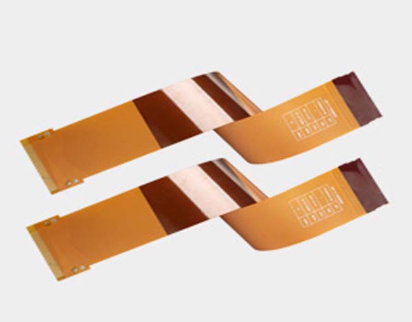
In addition to HDI technology, the integration of flexible and rigid-flex PCBs has also revolutionized custom PCB design.
Flexible PCBs, made from materials like polyimide, allow for bending and folding, which is ideal for applications requiring dynamic movement or unconventional shapes. Rigid-flex PCBs combine the benefits of both rigid and flexible circuits, offering enhanced durability and reliability. These innovations are particularly advantageous in industries such as aerospace, automotive, and medical devices, where flexibility and robustness are crucial.
Moreover, the advent of advanced materials and fabrication techniques has further propelled the capabilities of custom PCB design.
The use of materials such as ceramic and metal-core substrates has improved thermal management, a critical factor in high-power applications. Additionally, advancements in fabrication techniques, including laser drilling and precision etching, have enabled the production of PCBs with greater accuracy and complexity. These developments are essential for meeting the stringent performance and reliability requirements of modern electronic systems.
Another significant innovation in custom PCB design is the incorporation of embedded components.
By embedding passive and active components within the PCB substrate, designers can achieve a higher level of integration, reducing the overall size and weight of the device. This approach not only enhances the performance of the electronic system but also improves its reliability by minimizing the number of solder joints and interconnections. Embedded component technology is particularly beneficial in applications where space and weight constraints are critical, such as in aerospace and portable electronics.
Furthermore, the rise of digital design tools and simulation software has transformed the custom PCB design process.
These tools enable designers to create and test complex PCB layouts with greater efficiency and accuracy. By simulating the electrical, thermal, and mechanical behavior of the PCB, designers can identify potential issues early in the design phase, reducing the risk of costly errors and rework. This digital approach to PCB design is streamlining the development process, allowing for faster time-to-market and more innovative solutions.
In conclusion, the innovations in custom PCB board design technology are driving significant advancements in the electronics industry. From HDI and flexible PCBs to advanced materials and embedded components, these developments are enabling the creation of more efficient, compact, and reliable electronic devices. As technology continues to progress, the potential for further innovation in custom PCB design remains vast, promising exciting possibilities for the future of electronics.
Common Mistakes To Avoid In Custom PCB Board Design
Designing custom printed circuit boards (PCBs) is a complex process that requires careful attention to detail and a thorough understanding of both the technical and practical aspects involved. As engineers and designers embark on this intricate journey, it is crucial to be aware of common pitfalls that can compromise the functionality and reliability of the final product. By recognizing and avoiding these mistakes, one can ensure a more efficient design process and a successful outcome.
One of the most prevalent mistakes in custom PCB design is inadequate planning.
Before diving into the design phase, it is essential to have a comprehensive understanding of the project requirements, including the electrical, mechanical, and thermal constraints. Failing to establish clear objectives and specifications can lead to design iterations that are both time-consuming and costly. Therefore, investing time in thorough planning and documentation at the outset can significantly streamline the design process.
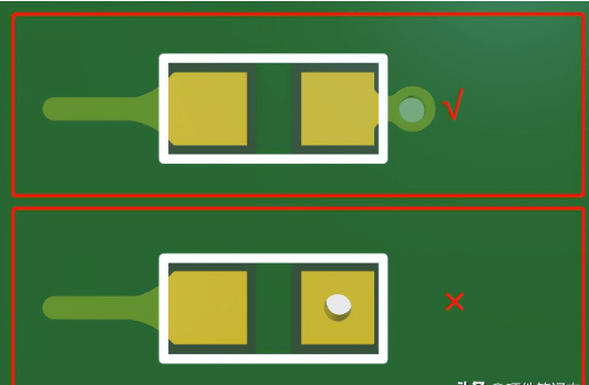
Another frequent error is neglecting to consider the manufacturability of the PCB.
Designers must be mindful of the capabilities and limitations of the fabrication process, as overlooking these factors can result in boards that are difficult or impossible to manufacture. This includes paying attention to design rules such as minimum trace widths, spacing, and hole sizes, which vary depending on the manufacturer. By collaborating closely with the fabrication team and adhering to their guidelines, designers can avoid costly redesigns and ensure a smoother production process.
In addition to manufacturability, signal integrity is a critical aspect that should not be overlooked.
Poor signal integrity can lead to issues such as crosstalk, electromagnetic interference, and signal degradation, which can severely impact the performance of the PCB. To mitigate these risks, designers should employ best practices such as proper trace routing, impedance matching, and the use of ground planes. Furthermore, conducting thorough simulations and analyses during the design phase can help identify potential signal integrity issues before they become problematic.
Thermal management is another area where designers often encounter challenges.
As electronic components become more powerful and compact, managing heat dissipation effectively is crucial to maintaining the reliability and longevity of the PCB. Designers should consider the thermal properties of materials, component placement, and the use of heat sinks or thermal vias to facilitate efficient heat transfer. By addressing thermal management early in the design process, one can prevent overheating and ensure optimal performance.
Moreover, component selection and placement are critical factors that can influence the success of a custom PCB design.
Choosing components that are readily available and have a long lifecycle can prevent supply chain disruptions and obsolescence issues. Additionally, strategic component placement can minimize trace lengths, reduce parasitic effects, and improve overall board performance. Designers should also be mindful of the mechanical constraints and ensure that components are placed in a manner that facilitates easy assembly and maintenance.
Lastly, inadequate testing and validation can lead to unforeseen issues in the final product.
It is imperative to conduct comprehensive testing at various stages of the design process, including design rule checks, electrical rule checks, and functional testing. By identifying and addressing potential issues early, designers can avoid costly rework and ensure that the PCB meets all performance and reliability requirements.
In conclusion, by being aware of and avoiding these common mistakes, designers can enhance the efficiency and success of their custom PCB board designs. Through meticulous planning, consideration of manufacturability, attention to signal integrity, effective thermal management, strategic component selection and placement, and rigorous testing, one can achieve a robust and reliable PCB that meets the desired specifications.