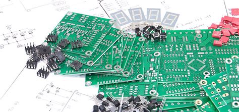
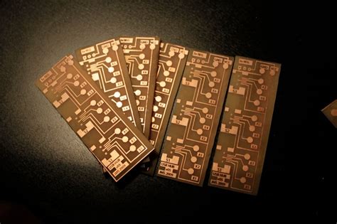
Custom PCB Manufacturing: Streamline Your Prototyping Process
Key Takeaways
Understanding critical factors in PCB manufacturing helps optimize both prototyping and full-scale production. When evaluating PCB manufacturing companies, prioritize those offering 24-hour rapid prototyping alongside transparent PCB manufacturing cost structures. Top-tier providers balance speed with rigorous quality checks, ensuring your design validation cycles stay on track without compromising reliability.
Implementing smart strategies can significantly reduce expenses. Consider these key comparisons:
| Factor | Prototyping Phase | Full Production |
|---|---|---|
| Turnaround Time | 24-48 hours | 2-4 weeks |
| Cost per Unit | Higher (low volume) | Lower (economies of scale) |
| Design Flexibility | High (iterative changes) | Limited (fixed designs) |
"Speed matters, but never at the expense of precision. Partner with PCB manufacturing businesses that validate designs through automated testing before scaling."
To maximize ROI, streamline workflows by integrating *DFM (https://www.andwinpcba.com) optimize fabrication processes.
By aligning your goals with a manufacturer’s capabilities, you accelerate innovation while maintaining control over budgets and timelines. Next, we’ll break down how rapid prototyping fuels agile development cycles.
Custom PCB Manufacturing Process Optimization
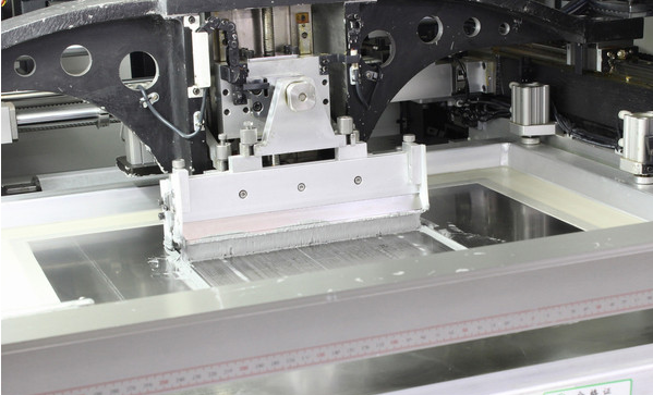
When optimizing your PCB manufacturing workflow, the goal is to eliminate bottlenecks while maintaining precision. Leading PCB manufacturing companies achieve this by integrating advanced design validation tools with automated production systems. By collaborating closely with your fabrication partner early in the design phase, you can identify potential issues—like impedance mismatches or thermal hotspots—before they escalate, reducing PCB manufacturing cost and turnaround time.
A key strategy involves standardizing design rules that align with your manufacturer’s capabilities. For instance, specifying consistent trace widths or avoiding overly complex via structures streamlines fabrication. Real-time feedback loops between your engineering team and the production floor ensure rapid adjustments, minimizing costly revisions. Additionally, leveraging just-in-time material sourcing prevents delays caused by supply chain disruptions.
To scale your PCB manufacturing business, prioritize technologies like panelization for bulk orders or modular tooling for flexible prototyping. Automated optical inspection (AOI) and electrical testing protocols further enhance quality control without sacrificing speed. Balancing these elements not only accelerates development cycles but also positions your projects for seamless transitions from prototype to full-scale production.

24-Hour Rapid Prototyping Solutions Explained
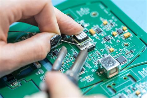
When developing custom electronics, time-to-market often dictates success. PCB manufacturing companies that offer 24-hour rapid prototyping enable you to compress design cycles while maintaining precision. By combining automated design verification with advanced fabrication technologies, these services eliminate traditional bottlenecks, turning your CAD files into functional prototypes within a single business day.
The process begins with rigorous DFM (Design for Manufacturability) checks to preempt errors, followed by high-speed laser drilling and multilayer stacking. Critical stages like solder mask application and surface finishing are optimized for speed without compromising the PCB manufacturing cost structure. For startups and enterprises alike, this accelerated approach reduces idle time between iterations, letting you validate designs faster and refine product features iteratively.
Leading providers integrate real-time tracking systems, so you can monitor progress and address issues mid-production. Whether you’re testing a high-frequency RF board or a dense IoT module, rapid prototyping ensures your PCB manufacturing business stays agile. The key lies in partnering with suppliers that balance cutting-edge equipment with domain expertise—ensuring even tight deadlines don’t sacrifice signal integrity or thermal performance.
By streamlining prototyping, you gain flexibility to experiment with complex layouts or novel materials, ultimately accelerating your path to full-scale production.
Cost-Effective PCB Production Strategies
When optimizing PCB manufacturing expenses, start by evaluating design complexity. Simplifying layouts reduces material waste and minimizes errors during fabrication—critical factors influencing long-term costs. Partnering with experienced PCB manufacturing companies allows you to leverage their expertise in material selection and process efficiency, ensuring you avoid over-engineering while maintaining performance.
Another strategy involves bulk ordering or panelization. By grouping multiple designs onto a single panel, you lower PCB manufacturing cost per unit, especially during prototyping phases. However, balance this with flexibility—modular designs let you scale production without redesigning entire boards.
Negotiate transparent pricing models with suppliers. Many providers offer tiered rates for higher volumes, aligning with your growth in the PCB manufacturing business. Additionally, consider alternative materials like FR-4 substitutes for non-critical applications, which can cut expenses by up to 20% without sacrificing reliability.
Finally, integrate Design for Manufacturability (DFM) checks early. Automated tools identify potential bottlenecks, reducing rework and delays. By aligning your workflow with these strategies, you maintain cost efficiency while preparing seamlessly for full-scale production—a logical next step in streamlining your development cycle.
From Prototype to Full-Scale PCB Assembly
Transitioning from prototype validation to full-scale production demands strategic alignment with your PCB manufacturing partner. While prototyping focuses on design verification, scaling requires addressing supply chain coordination, material sourcing, and assembly line optimization. Leading PCB manufacturing companies leverage automated workflows to minimize human error and maintain consistency across high-volume batches.
When evaluating PCB manufacturing cost at scale, consider factors like panelization efficiency and bulk material pricing. Advanced manufacturers often reduce per-unit expenses by optimizing board layouts for multi-project panels, ensuring you maximize ROI without compromising quality. Additionally, partnering with a PCB manufacturing business that offers integrated assembly services eliminates logistical bottlenecks, enabling seamless transitions from prototype testing to market-ready products.
This phase requires balancing speed with precision—automated optical inspection (AOI) systems and rigorous testing protocols ensure reliability in high-volume runs. By aligning your design requirements with your manufacturer’s capabilities early, you avoid costly redesigns and accelerate time-to-market. Whether you’re producing hundreds or millions of units, the right partnership transforms prototyping agility into scalable, repeatable success.
Expert Techniques for Accelerated PCB Development
To accelerate PCB manufacturing timelines without compromising quality, start by leveraging design standardization practices. Reusing proven circuit blocks and modular layouts reduces iterative revisions, allowing PCB manufacturing companies to focus on innovation rather than reinventing foundational elements. Pair this with automated design validation tools to flag potential fabrication issues early—saving weeks of rework.
Another critical strategy involves optimizing material selection for rapid prototyping. While advanced substrates may suit final products, using cost-effective, readily available materials during testing slashes PCB manufacturing cost and lead times. Collaborate with your fabrication partner to align material choices with both prototyping speed and end-use requirements.
For complex designs, adopt a phased verification approach. Break multi-layer boards into smaller, testable modules manufactured in parallel. This lets you validate functionality incrementally while maintaining momentum. Additionally, ensure your PCB manufacturing business adopts real-time data-sharing protocols—cloud-based design reviews and instant feedback loops eliminate bottlenecks that traditionally delay progress.
Finally, integrate design-for-manufacturability (DFM) guidelines from day one. Aligning your CAD outputs with your supplier’s equipment capabilities minimizes post-design adjustments. By combining these techniques, you transform PCB manufacturing from a linear process into a synchronized workflow, where speed and precision coexist.
Balancing Speed and Quality in Custom PCB Builds
When optimizing PCB manufacturing timelines, you can’t afford to treat speed and quality as opposing priorities. Leading PCB manufacturing companies achieve this balance by integrating advanced design-for-manufacturability (DFM) checks early in prototyping, ensuring errors are flagged before production begins. Automated optical inspection (AOI) and in-circuit testing (ICT) systems further streamline validation, reducing rework cycles while maintaining rigorous standards.
Your choice of materials and layer stackup directly impacts both PCB manufacturing cost and turnaround time. For instance, opting for FR-4 substrates over specialized laminates can cut lead times by 25% without sacrificing reliability for most applications. However, rushing through design reviews or skipping thermal simulations often leads to costly delays downstream. Instead, collaborate with your fabricator to align specifications with their production capabilities—this avoids over-engineering and keeps projects on schedule.
To sustain a competitive PCB manufacturing business, prioritize suppliers offering transparent pricing models and real-time progress tracking. Many now use AI-driven scheduling tools to allocate resources dynamically, ensuring 24-hour builds don’t compromise traceability or consistency. By balancing these strategies, you’ll minimize waste, accelerate time-to-market, and build prototypes that transition seamlessly to full-scale production.
Streamlined Workflows for PCB Design Innovation
Modern PCB manufacturing thrives on eliminating bottlenecks in design-to-production cycles. By integrating collaborative tools with PCB manufacturing companies, you can synchronize schematic updates, component placement, and layer stackup adjustments in real time. Cloud-based platforms, for instance, allow instant feedback loops between your team and fabrication partners, reducing revision cycles by up to 40%. This agility becomes critical when balancing tight deadlines with complex multilayer designs.
Automated design rule checks (DRCs) further refine workflows by flagging potential PCB manufacturing cost drivers early—like impractical trace spacing or undersized vias. Pairing these tools with modular prototyping services lets you validate iterations faster, ensuring that functional testing aligns with your product’s performance benchmarks. For PCB manufacturing business models prioritizing scalability, this approach minimizes wasted materials and labor hours during full-scale production.
Transitioning from prototyping to volume builds becomes seamless when your workflow accounts for manufacturability from day one. By aligning design software with your fabricator’s capabilities, you avoid costly redesigns while maintaining consistency across batches. The result? A unified process that accelerates innovation without compromising on the precision demanded by today’s electronics markets.
Maximizing ROI With Smart PCB Fabrication Choices
When selecting PCB manufacturing companies, you’re not just paying for boards—you’re investing in scalability, precision, and long-term value. To maximize ROI, begin by evaluating how PCB manufacturing cost aligns with your project’s lifecycle. High-volume orders often benefit from bulk pricing, but for prototyping, prioritize vendors offering flexible pricing tiers that adapt to iterative design changes.
Advanced PCB manufacturing partners integrate design-for-manufacturability (DFM) analysis, identifying potential flaws before production begins. This reduces costly re-spins and accelerates time-to-market—a critical factor in competitive industries. Consider hybrid approaches: use rapid-turn services for initial validation, then transition to full-scale production with optimized PCB manufacturing business solutions.
Material selection also impacts ROI. While FR-4 remains standard, high-frequency or thermal-sensitive designs may require specialized substrates. Partnering with PCB manufacturing companies that offer material libraries ensures you pay only for what your application demands. Finally, leverage automated quoting tools to compare lead times and costs transparently, transforming fabrication from a fixed expense into a strategic advantage.
Conclusion
Choosing the right PCB manufacturing partner transforms how you approach prototyping and production. By prioritizing speed, precision, and scalability, you ensure that your designs transition seamlessly from concept to functional boards. Leading PCB manufacturing companies leverage advanced technologies to reduce PCB manufacturing cost while maintaining stringent quality standards—critical for balancing tight timelines with reliable outcomes.
When evaluating your PCB manufacturing business needs, consider how rapid prototyping capabilities align with long-term production goals. A partner that offers flexible workflows not only accelerates iteration cycles but also minimizes waste, enabling you to allocate resources strategically. While cost-efficiency matters, investing in expertise that avoids costly redesigns or delays pays dividends over time.
Ultimately, the success of your projects hinges on aligning technical requirements with business objectives. As you refine your approach to PCB manufacturing, focus on partnerships that provide transparency, adaptability, and end-to-end support—key drivers for staying competitive in fast-paced markets.
FAQs
How do PCB manufacturing companies ensure quality in custom builds?
Reputable providers combine automated inspection systems with manual verification checks. You’ll typically see certifications like ISO 9001 and IPC-A-600 standards governing their processes, ensuring reliability even for complex designs.
What factors influence PCB manufacturing cost for prototypes?
Costs depend on board size, layer count, material selection, and turnaround time. For example, opting for FR-4 substrates over high-frequency materials reduces expenses, while 24-hour services may carry a premium.
Can PCB manufacturing workflows handle both small and large batches?
Yes—most businesses offer scalable solutions. Prototype orders often start at 5 units, while full-scale production runs can exceed 10,000 boards, with bulk pricing tiers improving cost efficiency.
How do you balance speed and quality in the PCB manufacturing business?
Leading companies use parallel processing—running design validation, material preparation, and fabrication simultaneously. This reduces lead times without compromising signal integrity or thermal performance.
What certifications should you prioritize when selecting a partner?
Look for ISO 13485 (medical), IATF 16949 (automotive), or UL listings for safety-critical applications. These ensure adherence to industry-specific compliance requirements.
Ready to Optimize Your PCB Project?
Explore tailored PCB manufacturing solutions designed for your needs. For instant quotes and expert guidance, please click here.