Custom PCB Printing and Assembly: Expert Techniques
Key Takeaways
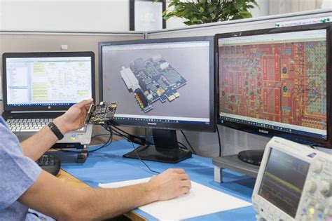
When navigating the complexities of custom PCB printing and assembly, understanding core principles ensures both technical precision and operational efficiency. For PCB assembly workflows, prioritizing automated optical inspection (AOI) and surface-mount technology (SMT) minimizes human error while accelerating production timelines. Advanced PCBA processes benefit from lead-free soldering alloys, which enhance durability while complying with global environmental standards.
Material selection remains pivotal—high-Tg laminates and low-loss substrates optimize performance in high-frequency applications, while thermal interface materials mitigate heat dissipation challenges. Rigorous quality control protocols, including in-circuit testing (ICT) and X-ray inspection, ensure reliability across batch productions.
Cost efficiency emerges through design-for-manufacturing (DFM) principles, which reduce material waste and streamline PCB assembly stages. Transitioning between design and production phases demands alignment with industry-standard certifications (e.g., IPC-A-610), ensuring consistency from prototyping to mass manufacturing. By integrating these strategies, manufacturers achieve a balance between precision, scalability, and long-term product viability.
Precision Custom PCB Printing
Achieving micrometer-level accuracy in PCB assembly begins with mastering photolithography and etching processes. Modern PCBA workflows leverage laser-direct imaging (LDI) systems to achieve trace widths below 25μm, ensuring compatibility with high-density interconnect (HDI) designs. Critical parameters include:
| Parameter | Standard Tolerance | Advanced Systems |
|---|---|---|
| Line Width | ±10% | ±3% |
| Layer Alignment | ±50μm | ±15μm |
| Dielectric Thickness | ±10% | ±5% |
Selective surface finishes like ENIG (Electroless Nickel Immersion Gold) or immersion silver enhance solderability while minimizing signal loss. For PCB assembly requiring impedance control, manufacturers employ vector network analyzers to validate characteristic impedance within 1% of target values.
This precision becomes especially critical when integrating embedded components or preparing for automated PCBA lines, where even minor deviations cause placement errors. Advanced shops combine automated optical inspection (AOI) with X-ray tomography to detect sub-surface voids or microcracks before panelization.
By optimizing these protocols, engineers reduce post-etch rework by 40% while maintaining signal integrity above 12GHz – a prerequisite for 5G and aerospace applications.
Efficient Assembly Techniques
Modern PCB assembly processes demand meticulous coordination between automated systems and precision engineering. At the core of PCBA efficiency lies the integration of high-speed pick-and-place machines, which reduce human error while accelerating component placement by up to 30,000 parts per hour. To optimize throughput, manufacturers employ dynamic thermal profiling during reflow soldering, ensuring consistent heat distribution across varied board geometries. This technique minimizes warping and solder joint defects, particularly in multi-layer designs.
A critical advancement in PCB assembly workflows is the adoption of inline automated optical inspection (AOI) systems. These tools perform real-time quality checks post-soldering, identifying misalignments or insufficient solder paste volumes before boards progress to testing phases. For mixed-technology assemblies, selective soldering systems enable precise application of solder to through-hole components without affecting adjacent surface-mount devices.
Design-for-manufacturing (DFM) principles further enhance efficiency by standardizing component orientations and spacing, reducing reprogramming delays during PCBA line changeovers. Additionally, modular fixturing solutions allow rapid reconfiguration for prototype batches or low-volume orders. By combining these strategies with just-in-time material sourcing, manufacturers achieve shorter lead times while maintaining defect rates below 0.5%. Such optimizations ensure that custom PCB printing and assembly projects balance speed, cost, and reliability across production scales.
Advanced Material Selection Guide
Selecting optimal materials for PCB assembly begins with understanding operational requirements and environmental factors. High-frequency applications demand substrates with low dielectric loss, such as Rogers RO4000 series, while industrial systems often prioritize thermal stability using FR-4 Tg170. For flexible circuits, polyimide films offer unmatched durability in dynamic bending scenarios.
Tip: Always cross-reference material datasheets with your PCBA design’s thermal expansion coefficients to prevent delamination during temperature cycling.
Copper weight directly impacts current-carrying capacity—2 oz/ft² copper is standard for power electronics, whereas 0.5 oz/ft² suffices for low-power signal layers. Surface finishes like ENIG (Electroless Nickel Immersion Gold) ensure solderability for fine-pitch components, while OSP (Organic Solderability Preservative) provides cost-effective protection for consumer-grade boards.
In high-reliability PCB assembly, halogen-free laminates meet RoHS compliance without compromising flame resistance. For RF/microwave designs, PTFE-based materials minimize signal loss above 10 GHz.
“Material compatibility with PCBA processes is non-negotiable—verify solder mask adhesion and drillability during prototyping.”
Advanced applications increasingly adopt metal-core substrates for LED lighting and automotive systems, where 8–12 W/m·K thermal conductivity prevents overheating. Hybrid builds combining FR-4 and ceramic-filled prepregs balance cost and performance in mixed-signal designs. Always conduct Tg (Glass Transition Temperature) testing under simulated operational stress to validate material choices.
Soldering Method Innovations Explained
Modern PCB assembly processes have undergone significant advancements in soldering techniques, driven by demands for higher reliability and miniaturization. Selective soldering has emerged as a preferred method for complex PCBA designs, enabling precise application of solder to specific components while minimizing thermal stress on sensitive parts. The integration of vapor phase reflow technology addresses challenges in heat distribution, particularly for boards with mixed-component densities, ensuring uniform temperature profiles during soldering.
Innovations in laser-assisted soldering now permit micron-level accuracy for ultra-fine-pitch components, reducing the risk of bridging or cold joints. Additionally, the adoption of low-temperature solder alloys (e.g., Sn-Bi-Ag compositions) enhances compatibility with heat-sensitive substrates without compromising mechanical strength. Automated optical inspection (AOI) systems paired with machine learning algorithms further refine quality assurance, detecting anomalies like insufficient fillets or tombstoning in real time.
For high-density interconnects, transient liquid phase sintering (TLPS) offers a void-free bonding solution, critical for aerospace and medical PCB assembly applications. These advancements collectively optimize yield rates and long-term durability, aligning with the industry’s shift toward scalable, error-resistant PCBA workflows.
Quality Control Best Practices
Effective quality assurance in PCB assembly (PCBA) begins with multilayered inspection protocols that address both design fidelity and manufacturing precision. Modern facilities employ automated optical inspection (AOI) systems to detect micron-level discrepancies in solder joints, component placement, and trace alignment, achieving defect rates below 50 parts per million. For high-reliability applications, electrical testing methods like flying probe and boundary scan validate circuit functionality under simulated operational loads.
Rigorous material verification ensures substrates and laminates meet IPC-4101 standards, with cross-sectional analysis confirming dielectric consistency and copper weight accuracy. In PCBA workflows, thermal profiling optimizes reflow soldering parameters, preventing tombstoning or cold joints while maintaining peak temperatures within ±2°C tolerances. Post-assembly, environmental stress screening (ESS) exposes boards to thermal cycling (-40°C to 125°C) and humidity exposure, identifying early-life failures before deployment.
Advanced manufacturers integrate statistical process control (SPC) dashboards to monitor critical-to-quality metrics in real time, enabling rapid adjustments to etching depths or solder paste deposition. Compliance with IPC-A-610 Class 3 requirements is non-negotiable for aerospace or medical-grade assemblies, mandating 100% X-ray inspection of BGAs and microvia integrity. By coupling these strategies with traceability systems that log component lot codes and machine calibration data, producers achieve first-pass yield rates exceeding 98.5% across complex PCB assembly projects.
Optimized Production Protocol Strategies
Implementing PCB assembly workflows with optimized production protocols requires balancing technical precision with operational efficiency. Central to this approach is the integration of real-time monitoring systems that track solder paste application accuracy and component placement tolerances during PCBA processes. Advanced facilities now employ machine learning algorithms to predict and compensate for thermal expansion variations, particularly when working with high-density interconnect (HDI) substrates.
A critical protocol involves dynamic scheduling models that automatically prioritize orders based on material availability and design complexity, reducing idle time between PCB assembly stages. For mixed-technology boards combining surface-mount and through-hole components, protocol optimization includes sequenced reflow profiles that prevent warping in multilayer configurations.
Quality assurance protocols have evolved to incorporate automated optical inspection (AOI) cross-referenced with 3D X-ray data, ensuring defect detection rates exceed 99.7% in modern PCBA lines. Leading manufacturers combine these technical measures with standardized documentation practices, creating traceable revision histories for every design iteration. This systematic approach not only accelerates time-to-market but also establishes reproducible benchmarks for complex projects requiring ISO 13485 or IPC Class 3 compliance.
Thermal Management in PCB Design
Effective thermal management is critical for ensuring the reliability and longevity of PCB assembly processes, particularly in high-density or power-intensive applications. As component miniaturization accelerates, managing heat dissipation becomes a central challenge in custom circuit board production. Designers often integrate thermal vias—plated holes that conduct heat away from sensitive components—and employ copper pours to create low-impedance paths for heat distribution.
In PCBA workflows, material selection directly impacts thermal performance. High thermal conductivity substrates, such as metal-core or ceramic-filled laminates, are increasingly preferred for applications requiring rapid heat transfer. Advanced soldering techniques, including void-free reflow profiles, further minimize hotspots by ensuring uniform thermal expansion across solder joints.
Proactive thermal analysis during the design phase—using simulation tools to model airflow and heat distribution—helps identify potential failure points before prototyping. Post-assembly, infrared thermography and thermal cycling tests validate design assumptions, ensuring compliance with industry standards like IPC-2221. For cost-sensitive projects, strategic placement of heat sinks or thermally conductive adhesives offers a balance between performance and manufacturing efficiency.
By aligning thermal management strategies with PCB assembly requirements, manufacturers can optimize both operational stability and product lifespan in demanding environments.
Cost-Effective Manufacturing Solutions
Achieving cost efficiency in PCB assembly requires a strategic balance between material optimization, process streamlining, and scalable production practices. Lean manufacturing principles play a pivotal role here, minimizing waste while maintaining precision in PCBA workflows. One effective approach involves adopting panelization techniques, where multiple circuit boards are grouped into a single panel during fabrication, reducing material waste and handling costs.
For high-volume projects, leveraging automated pick-and-place systems and reflow soldering not only accelerates production but also lowers labor expenses. Additionally, selecting standardized components over custom parts can yield significant savings without compromising functionality. Design for manufacturability (DFM) audits further ensure that layouts align with production capabilities, preventing costly redesigns or delays.
Suppliers offering bundled PCB printing and assembly services often provide volume discounts, particularly when using shared tooling or consolidated shipping. Implementing predictive maintenance schedules for equipment and adopting energy-efficient machinery also contribute to long-term cost reductions. Crucially, integrating automated optical inspection (AOI) early in the PCBA process helps identify defects before they escalate into expensive rework. By aligning these strategies with project-specific requirements, manufacturers can deliver competitively priced solutions without sacrificing the reliability expected in modern electronics.
Conclusion
In modern electronics manufacturing, the synergy between PCB assembly and precision printing forms the backbone of reliable circuit board production. As industries demand higher performance in compact designs, implementing advanced thermal management strategies becomes crucial alongside PCBA optimization. The integration of automated inspection systems and data-driven process controls ensures consistent quality while maintaining cost efficiency, particularly when scaling production.
Ultimately, success in PCB assembly hinges on balancing material innovation with process refinement—whether through low-temperature soldering techniques or high-frequency substrate selection. Manufacturers must remain agile, adapting to evolving standards like RoHS compliance and lead-free manufacturing requirements. By prioritizing cross-functional collaboration between design and production teams, businesses can achieve shorter lead times without compromising on signal integrity or durability.
Looking ahead, advancements in additive printing technologies and AI-powered defect detection promise to further revolutionize PCBA workflows, offering smarter solutions for prototyping and mass production alike. Staying ahead in this competitive landscape requires continuous investment in both skill development and equipment modernization, ensuring every custom board meets the exacting demands of tomorrow’s applications.
Frequently Asked Questions
What design considerations are critical for successful custom PCB assembly?
Key factors include proper component spacing, copper weight selection, and thermal relief patterns. Implementing DFM (Design for Manufacturing) guidelines ensures compatibility with automated pick-and-place systems, reducing PCBA errors by up to 40% in high-volume production.
How does material selection impact PCB reliability?
High-Tg FR-4 substrates and lead-free solders improve thermal stability in PCB assembly, while immersion silver finishes enhance signal integrity. For harsh environments, polyimide-based materials offer 3× better thermal cycling performance than standard options.
What quality control measures prevent defects in custom PCBA?
Automated optical inspection (AOI) and X-ray testing detect 99.7% of solder joint issues. Combining these with in-circuit testing (ICT) verifies electrical functionality, achieving <0.1% defect rates in mission-critical applications.
Why is thermal management crucial in modern PCB designs?
Improved heat dissipation through thermal vias and copper pours increases component lifespan by 25–30%. For high-power PCBA projects, ceramic-filled substrates reduce thermal resistance by 50% compared to traditional materials.
Can custom PCB manufacturing be cost-effective for prototypes?
Yes. Advanced panelization techniques and shared tooling reduce prototyping costs by 35–50%. Partnering with PCB assembly providers offering scaled pricing tiers optimizes budgets across development phases.
Explore Professional-Grade PCB Solutions
Refine your project’s technical specifications with industry-leading expertise—please click here to consult our PCBA engineering team for tailored manufacturing strategies.


