Custom PCBs: Revolutionizing Electronics Design and Manufacturing
Introduction
Printed Circuit Boards (PCBs) are the backbone of modern electronics. They provide the necessary platform for connecting and supporting various electronic components, enabling the functionality of devices ranging from smartphones to industrial machinery. While standard PCBs are widely available and used in many applications, the demand for custom PCBs has grown significantly in recent years. Custom PCBs offer tailored solutions that meet specific design requirements, providing enhanced performance, reliability, and flexibility. This article explores the world of custom PCBs, their benefits, design considerations, manufacturing processes, and their impact on various industries.
What are Custom PCBs?
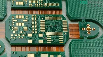
Custom PCBs are printed circuit boards that are specifically designed and manufactured to meet the unique requirements of a particular application. Unlike standard PCBs, which are mass-produced with generic designs, custom PCBs are tailored to the specific needs of a project, considering factors such as size, shape, layer count, material, and electrical performance.
Custom PCBs can range from simple single-layer boards to complex multi-layer designs with advanced features such as high-density interconnects (HDI), flexible circuits, and embedded components. The ability to customize these aspects allows engineers and designers to optimize the performance, reliability, and cost-effectiveness of their electronic devices.

Benefits of Custom PCBs
- Tailored Design: Custom PCBs are designed to meet the exact specifications of a project. This ensures that the board fits perfectly within the device, optimizing space utilization and improving overall design efficiency.
- Enhanced Performance: By customizing the layout, materials, and components, engineers can optimize the electrical performance of the PCB. This includes reducing signal interference, improving power distribution, and enhancing thermal management.
- Cost Efficiency: While custom PCBs may have higher upfront design costs, they can lead to significant cost savings in the long run. Custom designs can reduce the need for additional components, simplify assembly processes, and minimize the risk of design errors.
- Improved Reliability: Custom PCBs are designed with the specific application in mind, ensuring that the board can withstand the environmental and operational conditions it will encounter. This leads to improved reliability and longevity of the electronic device.
- Flexibility and Scalability: Custom PCBs offer the flexibility to incorporate new technologies and features as they become available. This scalability allows for future upgrades and modifications, extending the lifespan of the device.
Design Considerations for Custom PCBs
Designing a custom PCB requires careful consideration of various factors to ensure optimal performance and manufacturability. Some key design considerations include:
- Layer Count: The number of layers in a PCB depends on the complexity of the circuit and the required electrical performance. Single-layer boards are suitable for simple circuits, while multi-layer boards are used for more complex designs with high component density.
- Material Selection: The choice of PCB material affects the board’s electrical, thermal, and mechanical properties. Common materials include FR-4, polyimide, and ceramic. The material should be selected based on the application’s requirements, such as operating temperature, flexibility, and dielectric constant.
- Component Placement: Proper placement of components is crucial for optimizing signal integrity, thermal management, and manufacturability. Components should be arranged to minimize signal interference and ensure efficient heat dissipation.
- Routing and Trace Width: The routing of traces and the width of the traces affect the electrical performance of the PCB. Proper routing ensures signal integrity, while appropriate trace width helps manage current carrying capacity and heat dissipation.
- Thermal Management: Effective thermal management is essential for preventing overheating and ensuring the reliability of the PCB. This can be achieved through proper component placement, the use of thermal vias, and the selection of appropriate materials.
- Design for Manufacturability (DFM): Designing a PCB with manufacturability in mind helps reduce production costs and minimize the risk of errors. This includes considering factors such as panelization, solder mask application, and assembly processes.
Manufacturing Process of Custom PCBs
The manufacturing process of custom PCBs involves several steps, each of which must be carefully executed to ensure the quality and reliability of the final product. The key steps in the manufacturing process include:
- Design and Layout: The first step in manufacturing a custom PCB is the design and layout phase. This involves creating a schematic diagram of the circuit and translating it into a physical layout using PCB design software. The layout includes the placement of components, routing of traces, and definition of layers.
- Material Preparation: Once the design is finalized, the appropriate materials are selected and prepared. This includes the base material (substrate), copper foil, and solder mask. The materials are cut to the required size and cleaned to remove any contaminants.
- Printing the Circuit Pattern: The circuit pattern is printed onto the substrate using a process called photolithography. A photoresist layer is applied to the copper foil, and the circuit pattern is transferred using a photomask. The exposed areas of the photoresist are then developed, leaving the desired circuit pattern.
- Etching: The next step is etching, where the unwanted copper is removed from the substrate. The board is immersed in an etching solution that dissolves the exposed copper, leaving only the circuit traces protected by the photoresist.
- Drilling: Holes are drilled into the PCB to accommodate through-hole components and vias. The drilling process must be precise to ensure proper alignment and connectivity between layers.
- Plating and Coating: The drilled holes are plated with copper to establish electrical connections between layers. Additional coatings, such as solder mask and silkscreen, are applied to protect the board and provide labeling for components.
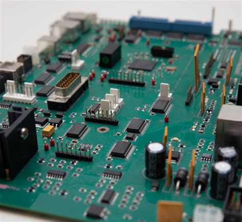
- Assembly: The final step is the assembly of components onto the PCB. This can be done using surface-mount technology (SMT) or through-hole technology (THT). The components are soldered onto the board, and the assembled PCB is inspected and tested for functionality.
Applications of Custom PCBs
Custom PCBs are used in a wide range of industries and applications, each with its own unique requirements. Some of the key applications include:
- Consumer Electronics: Custom PCBs are widely used in consumer electronics such as smartphones, tablets, and wearable devices. These devices require compact, high-performance PCBs that can accommodate a large number of components in a small form factor.
- Automotive: The automotive industry relies on custom PCBs for various applications, including engine control units, infotainment systems, and advanced driver-assistance systems (ADAS). Automotive PCBs must withstand harsh environmental conditions, such as temperature extremes and vibrations.
- Medical Devices: Custom PCBs are essential in medical devices, where reliability and precision are critical. Applications include diagnostic equipment, implantable devices, and patient monitoring systems. Medical PCBs must comply with strict regulatory standards and ensure patient safety.
- Industrial Automation: In industrial automation, custom PCBs are used in control systems, sensors, and robotics. These PCBs must be robust and reliable, capable of operating in demanding industrial environments.
- Aerospace and Defense: The aerospace and defense industries require custom PCBs for avionics, communication systems, and military equipment. These PCBs must meet stringent performance and reliability standards, often operating in extreme conditions.
- IoT and Smart Devices: The Internet of Things (IoT) and smart devices rely on custom PCBs to enable connectivity and functionality. These PCBs must be compact, energy-efficient, and capable of supporting wireless communication protocols.
Future Trends in Custom PCBs
As technology continues to advance, the demand for custom PCBs is expected to grow, driven by trends such as miniaturization, increased functionality, and the proliferation of IoT devices. Some of the key trends shaping the future of custom PCBs include:
- Miniaturization: The trend towards smaller, more compact devices is driving the need for custom PCBs with higher component density and advanced packaging techniques. This includes the use of HDI technology and embedded components.
- Flexible and Rigid-Flex PCBs: Flexible and rigid-flex PCBs are gaining popularity in applications where space and weight are critical. These PCBs offer the flexibility to conform to different shapes and can be used in wearable devices, medical implants, and aerospace applications.
- High-Speed and High-Frequency PCBs: With the increasing demand for high-speed data transmission and wireless communication, custom PCBs are being designed to support high-frequency signals. This requires careful consideration of signal integrity, impedance matching, and material selection.
- Sustainability: The electronics industry is increasingly focusing on sustainability, and custom PCBs are no exception. This includes the use of eco-friendly materials, recycling of PCB waste, and designing for energy efficiency.
- Advanced Manufacturing Techniques: Advances in manufacturing techniques, such as additive manufacturing (3D printing) and automated assembly, are enabling the production of more complex and high-quality custom PCBs. These techniques offer greater precision, flexibility, and cost-effectiveness.
Conclusion
Custom PCBs have become an essential component in the design and manufacturing of modern electronic devices. Their ability to be tailored to specific requirements offers numerous benefits, including enhanced performance, reliability, and cost efficiency. As technology continues to evolve, the demand for custom PCBs is expected to grow, driven by trends such as miniaturization, flexible circuits, and high-speed communication. By understanding the design considerations, manufacturing processes, and applications of custom PCBs, engineers and designers can leverage these versatile components to create innovative and high-performing electronic devices that meet the needs of today’s rapidly changing world.


