Deposition and etching techniques to reduce resistance of semiconductor metal lines
01 Introduction
The resistivity of copper is determined by its crystal structure, void volume, grain boundaries and material interface mismatch, and increases significantly with size reduction. Typically, the manufacturing process of copper wires is to etch trench patterns in low-dielectric silicon dioxide using a trench etching process, and then fill the trenches with copper through a Damascus process. However, this method will produce a polycrystalline structure with obvious grain boundaries and voids, thereby increasing the resistance of the copper wire. To prevent copper diffusion during the Damascus annealing process, a high-resistivity tantalum nitride lining material is also used in this process.
We can use physical vapor deposition (PVD) to deposit copper with high kinetic energy of 10 to 100 electron volts, resulting in a low-resistance, high-density single-crystal structure. However, the limitation of PVD is that it has poor coverage and can only be deposited uniformly on a flat surface, and cannot be used to fill deep holes or trenches (Figure 1a).
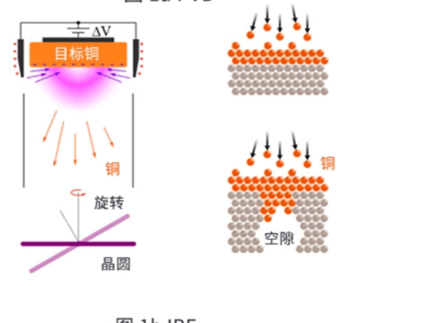
To get individual metal lines, you first need to deposit a uniform layer of copper on a flat surface, followed by physical etching with an ion beam.
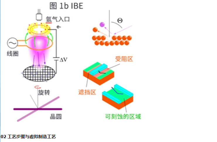
Copper does not produce volatile compounds with reactive gases, so reactive ion etching processes cannot be used. Accelerated argon ions produced in ion beam etching (IBE) can remove copper if the angle of incidence is very high. However, due to the blocking effect of the mask structure, the area that can be etched will be limited. Figure 1b shows the non-etchable area (red) when the mask is perpendicular to the incident ion beam, which is caused by the obstruction of the atomic ejection path caused by mask occlusion. When the mask is parallel to the ion path, all unmasked areas can be etched. Therefore, IBE is limited to etching linear masks of arbitrary length.
02 Process steps and virtual manufacturing process
To understand the impact of deposition and etching on wire resistance, we simulated the PVD and IBE processes using the SEMulator3D® visual deposition and etching functionality. With SEMulator3D, we reproduce PVD using a visibility deposition process with a 30° dispersion angle, which accurately simulates the random state of copper atoms and argon ions ejected during bombardment. At the same time, we simulated IBE using visible etching with a dispersion angle of 2° and a tilt angle of 60° to reflect the behavior of grid-accelerated ions with lower ion beam divergence.
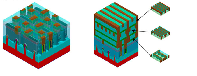
Both simulations treated the wafer as if it were freely rotating during the process, and other process steps were adjusted to accommodate the limitations of IBE and PVD. Figure 2 shows the same structure created using the Damascus copper filling process (Figure 2a) and the PVD/IBE process (Figure 2b). To accommodate some of the limitations of PVD/IBE and create the same shape for the desired final structure, additional process steps were added.
Experiments have proven that even with these limitations, equivalent 16nm SRAM (static random access memory) circuit cells can still be manufactured using PVD/IBE lines.
All metal layers above the middle of the line are made on a plane, so it is superior to the complex interconnect topology of FinFET (fin field effect transistor) devices and is an alternative to PVD/IBE metal lines. Figure 3 shows the independent structure of each metal layer and the necessary steps to create a three-layer metal FinFET structure using PVD/IBE.
Figures 3a and b show the independent structure of each metal layer and the necessary steps to create a three-layer metal FinFET structure using PVD/IBE.
Figure 3a: The left image shows a formed mid-end process 16nm FinFET structure, and the right image shows a FinFET structure with three complete metal layers. The surface is flat after the middle process, and copper PVD and IBE can be performed at this step.
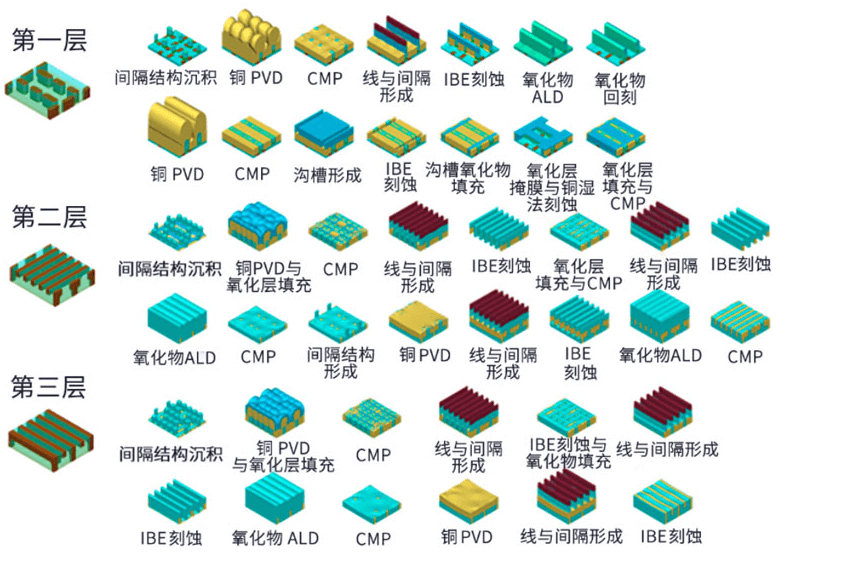
Figure 3b: This diagram shows the steps for fabricating each metal layer using PVD/IBE and demonstrates the process of exploring process and integration paths for fabricating three metal layers given the limitations of PVD and IBE. Each layer has corresponding diagrams to explain the manufacturing process step by step, and all partially involve columnar structure formation, copper PVD, chemical mechanical polishing (CMP), line and space formation, oxide filling, IBE etching, and atomic layer deposition (ALD). ), copper PVD and other independent process steps shown.
To form separate metal lines, spacers and mesas need to be fabricated to act as insulating barriers. After smoothing the deposit, patterning of lines and spaces can be performed, as well as etching of arbitrary lengths in the X or Y direction to create lines in the corresponding direction. When manufacturing through holes, cross etching can be performed to avoid cross etching of the line masks in the X and Y directions. Areas that do not require vias can be covered with insulating spacers before metal deposition.
03 Resistance results and conclusions
Subsequently, we measured the line resistance from the top metal to the P and N-channel vias of the FinFET structure under both Damascus process and PVD processes. Figure 4 shows the start and end points of P and N channel resistance measurements (all other insulating materials are transparent). In order to compensate for the contact resistance between the tantalum nitride lining layer and the copper wire, we considered the surface scattering effect of electrons when calculating the copper resistance. The closer to the tantalum nitride interface, the higher the copper resistivity. The attenuation length of the resistivity is set to 1nm. Because the Damascus-filled copper deposit is not expected to be fully crystalline, the resistivity of the copper increases by 50%. The PVD/IBE copper process does not use a tantalum nitride liner, so the exponential decay function is not applied and the bulk resistivity of copper is used in this model. Figure 4 contains a resistivity comparison table for the Damascus process and PVD.
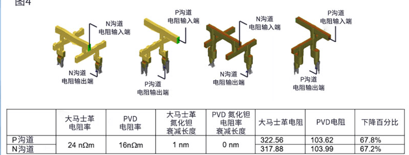
Figure 4 shows a 3D model diagram of a FinFET device using the Damascus process and PVD process. These models draw the resistance measurement points of the P and N channels. The table below the 3D model compares Damascus and PVD resistor values for P and N channel. The table shows that using IBE/PVD can reduce the resistance by 67% compared to Damascus deposition.
Resistance values calculated from the model show that the IBE/PVD fabrication method can reduce resistance by 67% compared to the traditional trench etching + Damascus deposition method. This is because IBE/PVD does not require a tantalum nitride lining layer and the copper wire resistivity is low during the process. This result shows that IBE/PVD can reduce resistivity during metal wire manufacturing compared to Damascus filling, but at the expense of a more complex manufacturing process.


