Design and Implementation of Unknown Circuit Board Schematic Mapping System
In recent years, my country has introduced a large number of advanced instruments and equipment, which are large in size, complex in structure and highly integrated. After years of use, these equipment have encountered great difficulties in maintenance, repair and spare parts guarantee. Since it is not a technology introduction, there is almost no technical information about the equipment, and the circuit schematic of the electronic spare parts cannot be obtained. Therefore, the mapping of the circuit schematic of the unknown (no circuit schematic) circuit board is of great significance for the reverse design of electronic spare parts, especially military products.
1 Basic Principles
To complete the reverse design of unknown electronic spare parts, you must first know the connection table of the spare part, and then draw the original circuit schematic based on the relevant knowledge of the component database, and then form an alternative plan through technical analysis and design to achieve reverse design. There are two common methods for mapping unknown circuit boards:
(1) Use the ohmmeter of a multimeter to perform connection tests on the exposed solder joints and component pins on the printed circuit board, that is,
first measure the resistance between the first solder joint (or pin) and the second and third solder joints (or pins), until all solder joints and pins are measured, thereby obtaining the connection diagram of the first solder joint or pin on the circuit board. Use the same method to measure the resistance between the second solder joint (or pin) and the third and fourth solder joints (or pins), until all solder joint pins are measured, thereby obtaining the connection diagram of the second solder joint or pin on the circuit board. By analogy, the connection relationship between each solder joint and component pin on the circuit board (i.e., network diagram) can be obtained. Although this method can obtain the network diagram of the circuit board, it is very cumbersome, inefficient, and has a high error rate. Therefore, automatic mapping equipment should be developed.
(2) Use a fixed needle bed to measure and map.
For each circuit board, a special test needle bed is designed. The special needle bed is reliably contacted with all the contacts of the circuit board to be tested. Under the control of the computer test software, the test can be completed in a short time through a special channel controller, and the multi-layer circuit board can be measured and mapped. However, this method requires a special needle bed and test software to be designed for each object to be tested, which has high investment costs and long cycles.
Combining the advantages of the above two methods, according to the commonly used path resistance test method, a “flexible needle bed network diagram mapping system” was designed to achieve flexible and efficient mapping. After the connection table test is completed, the circuit schematic can be drawn by manual intervention with the help of a specially established device database.
2 System hardware design
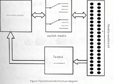
2.1 Overall system structure
The system consists of a computer, a switch matrix, a flexible needle bed array and spare parts to be tested. Its structure is shown in Figure 1. Among them, the flexible needle bed array is reliably connected to all nodes on the circuit board through flexible needles, and the switch matrix realizes automatic switching or sequential switching of channels. The width of the flexible needle bed can only cover one electronic chip, so that the entire circuit board to be tested can be covered by multiple needle beds.
During the test, the circuit board is fixed horizontally, and the flexible needle bed is fixed horizontally at a spacing of 2 to 3 cm above and below the circuit board. There are densely distributed solder joints on one side of the flexible needle bed. These solder joints are connected to the exposed solder joints or component pins on one side of the circuit board to be tested through elastic probes with variable lengths. The other side of the flexible needle bed is connected to each solder joint with the switch matrix by a wire, and the same operation is performed on the other side of the circuit board, so that the exposed solder joints or component pins of the circuit board are led to the flexible needle bed, and the switch matrix is controlled by a computer to realize the automatic test of the connection relationship between each node on the flexible needle bed.
2.2 Test circuit structure composition
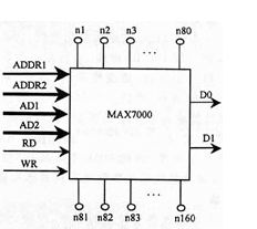
This system adopts a custom bus structure. Each flexible needle bed is connected through a bus, and the communication between them is controlled by the control module. The test circuit is connected to the host through a USB bus interface, as shown in Figure 2.
Among them, ADDR1 and ADDR2 are the needle bed address buses, and the control module implements the addressing of the needle bed by sending the corresponding address code. Since it is necessary to test between the needle bed itself and the two needle beds during testing, only one set of address buses cannot address the two needle beds at the same time, so two sets of address buses ADDR1 and ADDR2 are designed to address the two test needle beds at the same time.
RD and WR are read enable and write enable buses.
When RD is valid, the test needle bed is allowed to send data to the control module. When WR is valid, the control module is allowed to send instructions to each needle bed to realize the control function.
AD1 and AD2 are the needle bed control needle address buses.
Since each probe needs to be traversed with other probes during testing, two sets of address buses are designed to address two different probes at the same time. The probe signal addressed by AD1 is led out through the data line D1, and the probe signal addressed by AD2 is led out through the data line D2. By measuring the resistance between D1 and D2, the connection between the corresponding circuit board solder joints can be obtained.
In this design, the PC controls the tester through the USB interface, and the test data is sent back to the PC through the USB interface for analysis. The analysis results are used to diagnose the faults of the UUT.
This system uses Cypress’s AN2131QC as the controller chip. Figure 3 shows a simplified block diagram of the structure of AN2131QC. The USB bus transceiver is connected to the USB bus pins D+ and D-. The serial interface engine is used to decode and decode the serial data, error check, bit fill, and complete the signals required by other USB buses, and finally realize the data transmission with the USB bus interface. The general microprocessor uses the enhanced 8051, which has faster execution speed and more powerful functions compared with the standard 8051. RAM is used internally as program code and data storage, so the 8051 sequence has a “soft” feature, that is, the user can automatically load code and data to implement specific functions.
2.2.2 Control module
The control module is used to complete the addressing, control, testing, and data sending and receiving functions of each needle bed. The host issues control commands and receives data through the USB interface. The control module structure is shown in Figure 4.
The system control chip uses ALTERA’s MAX7000 series programmable logic device (CPLD), which is used to receive control signals sent by the host, control the test circuit, receive test data and upload it to the host. When WR is valid, the control instruction is received; when RD is valid, the test data is received. There are five test signals on the test circuit custom bus, so three control signal lines A, B, and C are used, and different control signals can be output after decoding. The resistance test circuit is also located in the control module, which is responsible for testing the two solder joints (or pins) of the circuit board led out by D1 and D2. The test results are sent to the host by the CPLD after A/D conversion.
2.2.3 Test needle bed
The test needle bed is used to connect each solder joint or pin of the circuit board with probes, and use the switch matrix to automatically switch the connection between each probe, so as to realize the interconnection test between each solder joint. The needle bed circuit is shown in Figure 5.
The switch matrix is implemented using MAX7000 series programmable logic devices, which are used to connect all probes on the needle bed, receive control signals and output the addressed probe signals.
3 System software design
The system software runs on the PC platform, controls the test circuit through the USB bus and receives the test circuit test data, and forms the circuit connection table of the tested circuit board according to the received data. Now we mainly analyze the test circuit control program related to circuit mapping:
(1) First, use ADDR1 to address the test reference needle bed.
Each needle bed has a specific address code. For example, sending ADDR1=00000001 means that the test needle bed No. 1 is selected, and this is used as the reference test needle bed to test other needle beds.
(2) The test needle bed No. 1 uses the AD1 bus to address all the probes on it.
The AD1 bus addresses the reference test point of the needle bed. For example, sending AD1=00000001 means that the probe No. 1 is addressed, that is, the probe No. 1 is connected to the D1 terminal.
(3) Using the needle bed addressed by ADDR1 as the reference, use ADDR2 to address all needle beds, and use the AD2 bus to address the probes on the addressed needle beds.
(4) Using the probes addressed by the AD1 bus as the reference, perform traversal testing on the probes addressed by the AD2 bus.
The pseudo code of the program is as follows:
for(ADDR1=1 to 20) //Assume that there are 20 test needle beds in total, select the benchmark test needle bed
{
for(AD1= 1 to 256) //Assume that each needle bed has 256 probes connected to solder/points, select the benchmark test solder point
{
for(ADDR2=1 to 20) //Address all needle beds in sequence
{
for(AD2= 1 to 256) //Address all probes (solder points) on the test needle bed in sequence
{
//Test circuit test function
…
}
}
}
}
Through the above test program, the traversal test of each probe (solder point) and all other probes (solder points) can be realized, so as to obtain the connection status of each solder point on the circuit board.
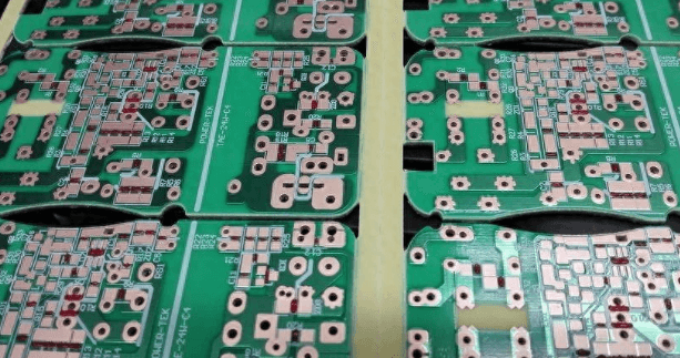
Through the knowledge of component models on the circuit board, using the circuit board connection table mapped by this set of mapping system, combined with the corresponding PCB design software and manual intervention, the mapping of unknown circuit boards was realized on a certain imported equipment, and its circuit schematic diagram was obtained, laying the foundation for the next step of reverse design work. Due to the intellectual property rights involved, this system is only applied to electronic devices in special fields.


