Design basis of printed circuit boards
Design basis of printed circuit boards
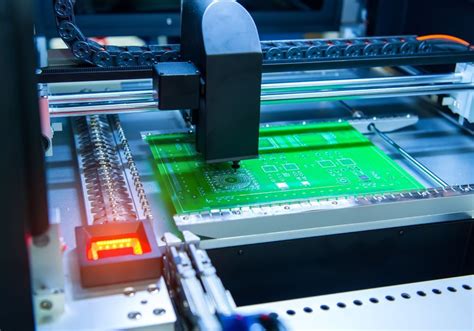
The circuit design ideas of electronic designers must eventually be implemented in reality, that is, printed circuit boards. The substrate and selection of printed circuit boards, the physical properties of the various elements that make up the circuit, such as vias, slots, wire sizes, pads, surface coatings, etc., are factors that designers must consider when designing. This is the basis for designing high-quality printed circuit boards and the most critical part of printed circuit board processing.
1 Substrate for printed circuit boards
1.1 Copper foil substrate for rigid printed circuit boards
⑴ Phenolic paper laminates
Phenolic paper laminates can be divided into different grades. Most grades can be used at temperatures as high as 70℃~105℃. Long-term operation at temperatures above this range may lead to some performance degradation (but this still depends on the grade and thickness of the substrate), and overheating will cause carbonization. In the affected area, the insulation resistance may drop to a very low value. Such a heat source is a heating element. Within the normal temperature range, the substrate may undergo severe blackening (sunlight can also make the substrate black, but it will not cause changes in material properties). Placing it in a high humidity environment will greatly reduce the insulation resistance of the substrate, but when the humidity decreases, the insulation resistance will increase again.
⑵ Epoxy paper laminate
Compared with phenolic paper laminate, epoxy paper laminate has greatly improved electrical and non-electrical properties, and has better mechanical processing and mechanical properties. Depending on the thickness of the material, its use temperature can reach 90℃~110℃.
⑶ Polyester glass felt laminate
The mechanical properties of polyester glass felt laminate are lower than those of glass cloth-based materials, but higher than those of paper-based materials. However, it has good impact resistance and good electrical properties, can be used in a wide frequency range, and can maintain good insulation properties even in high humidity environments. Its use temperature can reach 100℃~105℃.
⑷ Epoxy glass cloth laminate
The mechanical properties of epoxy glass cloth laminate are higher than those of paper-based materials, especially the bending strength, impact resistance, warping and resistance to welding heat shock are better than those of paper-based materials. This material also has good electrical properties, can be used at temperatures up to 130°C, and is less affected by harsh environments (humidity).
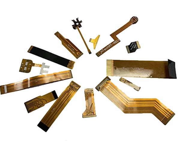
1.2 Copper foil substrate for flexible printed circuit boards
⑴ Polyester film
The most commonly used property is flexibility, and its characteristic is that it can form a retractable coil when heated. If a suitable adhesive is used, this material can be used in the range of 80°C to 130°C. Special attention should be paid during welding, as this material is prone to softening and deformation at welding temperatures. It has excellent electrical properties and can maintain its good electrical properties when exposed to high humidity environments.
⑵ Polyimide film
Polyimide film has good flexibility and can remove absorbed moisture through preheating to ensure safe welding. Generally, adhesive polyimide film can work continuously at temperatures up to 150°C, special accommodative polyimide film using fluorinated ethylene propylene as an intermediate film and used at 250°C, and polyimide film without adhesive for special purposes can be used at higher temperatures. Polyimide film has excellent electrical properties, but may absorb moisture and affect performance.
⑶ Fluorinated ethylene propylene film
Fluorinated ethylene propylene film is usually combined with polyimide or glass cloth to make a laminate, and has good flexibility and stability at a welding temperature not exceeding 250℃. It can also be used as a non-support material. Fluorinated ethylene propylene film is a thermoplastic material with a melting temperature of about 290℃. It has good moisture resistance, acid resistance, alkali resistance and organic solvent resistance. Its main disadvantage is that the conductive pattern is prone to movement at the lamination temperature during lamination.
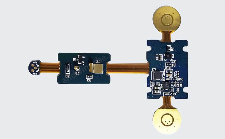
1.3 Rigid-rabbit combined printed circuit board
If the same printed circuit board includes both flexible and rigid parts, that is, the materials used for rigid printed circuit boards, the materials used for flexible printed circuit boards and the materials used for multilayer printed circuit boards can be combined in the same structure, but some properties may change significantly due to the different adhesives used.
2 Vias
The ratio of board thickness to hole diameter should preferably be greater than 3:1. A large ratio will make production difficult and increase costs. When vias are used only for through-hole connections or inner-layer connections, the aperture tolerance, especially the minimum aperture tolerance, is generally unimportant and therefore need not be specified. Since no components are inserted into the via hole, its aperture can be smaller than the aperture of the component hole.
When vias are used as component holes, the minimum aperture of the via should be adapted to the pin size of the component or assembly. Designers should use the given nominal aperture as the recommended value for vias. The maximum aperture of the via depends on the plating thickness and the tolerance of the aperture. The minimum plating thickness of the specified hole is generally allowed to deviate by 10% (hole to hole). It is recommended that the average thickness of the copper plating on the hole wall should not be less than 25μm (0.001in), and the minimum thickness should be 15μm (0.0006in).
3 Wire size
3.1 Wire width
For special designs or layouts of conductive patterns, the wire width should usually be as wide as possible, at least wide enough to withstand the expected current load.
The accuracy of the conductor width available on a printed board depends on production factors, such as the accuracy of the production substrate, the production process (printing method, use of additive or subtractive processes, plating method, etching quality) and the uniformity of the conductor thickness. The specified conductor width includes the design width and the allowed deviation, as well as the specified minimum line width. Deviations caused by gaps, pinholes or edge defects, although not included in these deviations, will also appear. When the conductor width reduction caused by these defects does not exceed a certain value of the relevant specifications, it is usually acceptable, and this value ranges from 20% to 35%. If the required current carrying capacity is high, these defects must be taken into account.
3.2 Conductor spacing
The spacing between adjacent conductors must be wide enough to meet the requirements of electrical safety, and the spacing should be as wide as possible for ease of operation and production. The minimum spacing selected should be suitable for the applied voltage. This voltage includes repeated or occasional overvoltages or peak voltages during normal operation or failure. Therefore, the conductor spacing should meet the safety requirements to be adopted or specified.
If the relevant specifications allow the presence of metal particles between conductors, the effective conductor spacing may be reduced. When considering voltage issues, any reduction in spacing due to metal particles between conductors should be taken into account.
If the conductor spacing exceeds a certain value, it will be beneficial to operation and production. In some cases, it is easy to meet practical requirements by only specifying the minimum limit. If the minimum limit of the conductor width is specified, the minimum limit of the conductor spacing must also be specified. If metal particle defects exist between the conductors, the specified minimum conductor spacing should be increased. The designed inner layer conductor or pad should be more than 2mm away from the edge of the board.
4 Pad size
All component holes are electrically connected through pads. In order to facilitate maintenance, a strong bond with the substrate should be ensured, and the pads around the holes should be as large as possible and meet the welding requirements. Usually non-vias are larger than the pads required for vias. On double-sided printed boards with vias, each via for the conductor terminal should have a double-sided pad. When the via is located on the conductor, the via is filled with solder during the overall welding process, so no pad is required. It is the responsibility of the design engineer to ensure that the conductors around the hole meet the design current requirements and meet the process requirements of the position tolerance related to production. When the via is located on the conductor without a pad, the printed circuit board manufacturer should be provided with a method to identify the center of the hole.
In order to facilitate the overall welding operation, large areas of copper foil should be avoided. And in accordance with the design principles, the pads on the component side and the welding side are preferably placed symmetrically (relative to the hole).
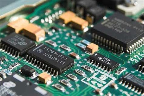
5 Metal plating (coating) coating
Metal plating (coating) coating is used to protect the metal (copper) surface and ensure its solderability. It can also be used as an anti-corrosion layer for etching liquid in some processing processes (such as in the processing of holes). Metal plating (coating) coating can also be used as the contact surface between the connector and the printed circuit board, or the bonding layer between the surface mounted device and the printed circuit board.
A plating layer suitable for the conductive pattern should be selected according to the purpose of the printed circuit board. The type of surface plating layer directly affects the production process, production cost and performance of the printed circuit board.
6 Printed contact sheet
When using printed contact sheets, care should be taken to select a plating layer that is compatible with the plating on the matching corresponding contact. Since the selection of a suitable plating layer is related to the following factors, there is no general rule to follow. The contact surface of the printed metal sheet should be smooth and free of defects that could cause degradation of electrical and mechanical properties.
7 Nonmetallic Coatings
7.1. Nonmetallic Coatings
Nonmetallic coating materials are used to protect printed boards. In addition, solder resist areas are used to prevent solder wetting of non-solder area conductors.
Improper cleaning may result in reduced adhesion when the coated assembly is exposed to high humidity conditions. Due to reduced adhesion, separation points or debris begin to appear at the interface between the coating and the substrate, and peeling (“erosion”).
Before applying any coating, it is most important to properly clean the printed board. If the printed board has organic or inorganic contamination, its insulation resistance cannot be improved by the coating.
If the coating is not selected and used correctly, it may result in reduced parameters such as flame retardancy, insulation resistance, and electrical performance of the printed board used at high frequencies.
7.2 Temporary Protective Coatings
Temporary coatings can be used to protect the solderability of conductive patterns. Temporary protective coatings are usually applied to conductive patterns covered by metal coatings that do not have good solderability to maintain good solderability for the necessary time.
Depending on the material used, temporary protective coatings can be removed before soldering or can act as flux. Temporary protective coatings that act as flux are resin-based and soluble in flux solvents.
Excessive drying and/or long-term storage, or excessive heating (for example, when the printed board is subjected to vapor phase soldering), may cause some resin-based coatings to solidify at a point where the coating is no longer fully dissolved in the short time between the application of flux and soldering, thereby reducing the soldering effect.
Usually, the resin-based coating is thinnest at the intersection of the hole wall and the pad. Over time, the solderability of the via may decrease faster here than in other areas.
For the above reasons, the coating should be compatible with the process to be implemented. For example, drying, fluxing, soldering and heat-melting methods must be carefully considered.
7.3 Temporary solder resist
Coatings using temporary solder resist are usually applied by screen printing before soldering. Covering a specified area of a printed circuit board to prevent solder wetting of the conductive pattern in that area. For example: a temporary solder resist is applied to a circuit area with precious metals as a surface coating. In addition, this coating can protect the coated area from damage during the production process and storage process.
After completing the protection task, the temporary solder resist should be removed. Depending on the type of solder resist used, it can be peeled off or soaked in a suitable solvent. It should be noted that the temporary coating must be completely removed.
8 Permanent protective coating
Permanent protective coatings can improve or maintain the electrical properties of printed circuit boards, such as insulation resistance and breakdown voltage between conductors on the surface of printed circuit boards. They usually contain strong scratch-resistant materials to protect the board from damage. In normal use, they remain on the printed circuit board permanently.
Permanent protective coatings can improve or maintain the electrical performance of printed boards by:
⑴ Preventing moisture from entering the substrate;
⑵ Preventing dirt from depositing between wires (such as moisture-absorbing dirt);
⑶ Acting as an insulating material between wires;
⑷ Acting as a protective layer inside or on the surface of vias (through holes) that do not require soldering.
This coating is applied before the soldering operation to cover the specified area of the printed board to prevent solder wetting of the conductive pattern in that area. Unlike stripping or washing type temporary coatings, permanent solder resist cannot be removed after the soldering operation, but acts as a permanent protective coating. When used as a solder resist, it should have sufficient protective properties in addition to the above electrical properties.
9 Conformal coatings
Conformal coatings are an electrically insulating material applied to printed boards or printed board assemblies as a protective barrier to block the effects of harmful substances in the environment. If selected and applied properly, conformal coatings will help protect assemblies from moisture, dust and dirt, airborne contaminants (e.g., smoke, chemical gases), conductive particles (e.g., metal flakes, metal shavings), accidental shorts caused by dropped tools and fasteners, wear damage, fingerprints, vibration and shock (to some extent), and mold growth.
The selected conformal coating resin should meet these requirements and some other secondary requirements, such as transparency (the value of the component should be identifiable after coating) and flexibility (to prevent damage to the component during high and low temperature cycles).
In some cases, certain lacquers are used as permanent protective coatings. Such lacquers are applied after soldering and usually only on the soldering surface.
In addition to their protective properties, conformal coatings also have other special properties. For example, they are fluorescent, which facilitates visual inspection of coverage.
Some limitations of using conformal coating resins are:
① Conformal coating films are permeable to water vapor, and formulations that do not contain corrosion-resistant fillers (such as chromates) will not prevent corrosion caused by electrolytic salts applied to parts during the coating process or salts captured on the surface of parts.
② Conformal coating films are permeable to water, and as the thickness of the film increases, the insulation resistance will decrease. Especially the resin edges around components (such as integrated circuits).
③ Organic conformal coating resins are used to fill gaps between wires, which will cause significant changes in inter-wire capacitance.
④ Transparent and flexible conformal coating resins have a high coefficient of thermal expansion, so they may produce lifting forces on some components, causing solder joint failure.
⑤ Conformal coating resins used to improve electrical performance do not contain adhesive formulations that improve adhesion (such as phosphates), so they cannot provide additional adhesion to metals, especially to solder.
10 Dimensions of printed circuit boards
Be careful to avoid unnecessary tight dimensional tolerances, otherwise it will make production difficult and increase costs. For production or inspection purposes, it is recommended that reference datums be used to determine the size and position of graphics. If a printed board contains more than one graphic, all graphics should use the same reference datum. The reference datum is preferably specified by the designer. A common method is to use two orthogonal lines.
In some cases, the location of each processing feature may require the use of more than one reference datum. This may occur on very large boards or on rigid-flex printed boards with two or more rigid areas. The dimensions and tolerances between reference datums depend on the materials used and the dimensional requirements of the finished board.
10.1 Board Dimensions
In principle, the board can be of any shape, but simple shapes are more conducive to production.
Unless the number of processes justifies some special production methods, the size of the printed board is usually limited by the production equipment and stability requirements.
The board can reach
The tolerances on the dimensions of the printed board are usually the same as those achievable with laminated materials because the tolerances of the substrates used are similar.
10.2 Board Thickness
Requirements for substrate thickness, board thickness, or total board thickness shall be limited to the specified thickness control area of the printed board. Dielectric thickness is defined as the minimum distance measured between adjacent conductive layers.
When additional plating, coating, covering, or adhesives are used, the total board thickness will deviate from the thickness requirements of the metal foil-clad substrate, and all dimensional tolerances shall be as loose as possible.
10.3 Hole Size
From an economic point of view, the number of holes of different sizes should be kept to a minimum in any design.
10.4 Bending of Flexible Printed Boards
The bending area should be minimized. Vias and areas for mounting components should not be set in the bending area. The conductor material is rolled and cannot change the direction of the bend line. The conductor in the bend area should cross the bend line perpendicularly or obliquely.
The bending radius should be as large as possible. The allowable bending radius depends on the conductor thickness, substrate thickness, and thickness of the finished flexible printed board. The conductor should be as symmetrical as possible with the central axis of the flexible printed circuit board structure.
The warpage of the printed circuit board is related to the materials used, production process, hole pattern, uniformity of conductive pattern distribution, size and type of the printed circuit board, etc.
11 Selection of printed circuit board substrate
In addition to providing the structure required for assembly, the substrate also provides the leads and heat dissipation required for power supply and electrical signals. Therefore, a good substrate should have the following functions:
① Sufficient mechanical strength (with distortion, vibration and impact, etc.);
② Able to withstand heat treatment and impact in the assembly process;
③ Sufficient flatness to suit automated assembly process;
④ Able to withstand multiple rework (welding) work;
⑤ Suitable for PCB manufacturing process;
⑥ Good electrical properties (such as impedance, dielectric constant, etc.).