Design of a Heart Rate Monitoring PCB for Exercise Training
Abstract
This paper presents a comprehensive design approach for a printed circuit board (PCB) that monitors heart rate during physical exercise. The system integrates photoplethysmography (PPG) sensors, signal conditioning circuitry, microcontroller processing, and wireless communication capabilities to provide real-time heart rate data for fitness enthusiasts and athletes. The design considerations include power efficiency, motion artifact reduction, signal integrity, and user interface implementation. The resulting PCB offers a cost-effective solution for exercise heart rate monitoring with potential applications in wearable fitness technology and sports performance tracking.
1. Introduction
Heart rate monitoring has become an essential tool for athletes, fitness enthusiasts, and healthcare professionals to optimize training intensity, track cardiovascular health, and prevent overexertion. Modern exercise physiology emphasizes the importance of maintaining specific heart rate zones for different training objectives, making accurate real-time monitoring crucial.
Traditional chest strap monitors, while accurate, can be uncomfortable during prolonged use. This paper describes the design of a wrist-worn or arm-mounted PCB that provides comparable accuracy with improved wearability. The design focuses on:
- High signal-to-noise ratio for reliable readings during movement
- Low power consumption for extended battery life
- Compact form factor for wearability
- Wireless connectivity for data logging and analysis
2. System Architecture
The heart rate monitoring PCB consists of several key subsystems:
2.1 Optical Sensor Module
The core sensing technology uses photoplethysmography (PPG), which detects blood volume changes in peripheral capillaries by measuring light absorption. The module includes:
- Green LED (typically 525nm) for optimal blood absorption characteristics
- Photodiode with appropriate spectral sensitivity
- Optical window design to maximize signal quality
2.2 Analog Front-End
The weak photodiode signal requires careful conditioning:
- Transimpedance amplifier to convert current to voltage
- Programmable gain amplifier (PGA) to adjust for skin tone variations
- Active bandpass filter (0.5Hz to 5Hz) to isolate pulse waveform
- 24-bit ADC for high-resolution signal digitization
2.3 Digital Processing Unit
A low-power microcontroller handles:
- Real-time signal processing algorithms
- Heart rate calculation (beats per minute)
- Motion artifact compensation
- User interface control
2.4 Power Management
Efficient power delivery is critical for wearable devices:
- Lithium polymer battery (3.7V nominal)
- Switching regulators for multiple voltage rails
- LED driver with pulse modulation for power savings
- Low-power sleep modes between measurements
2.5 Wireless Communication
Bluetooth Low Energy (BLE) enables:
- Real-time data streaming to smartphones
- Firmware updates
- Configuration changes
3. PCB Design Considerations
3.1 Stackup Design
A 4-layer PCB provides optimal signal integrity:
- Top Layer: Components and signal routing
- Inner Layer 1: Ground plane
- Inner Layer 2: Power distribution
- Bottom Layer: Additional routing and shielding
3.2 Component Placement
Strategic component placement minimizes noise:
- Keep analog and digital sections physically separated
- Position sensitive analog components away from RF sources
- Place decoupling capacitors close to IC power pins
- Optimize LED-photodiode optical path
3.3 Routing Guidelines
Careful routing preserves signal quality:
- Minimize analog trace lengths
- Use guard rings around high-impedance nodes
- Maintain consistent impedance for digital lines
- Avoid right-angle turns in sensitive traces
3.4 Grounding Scheme
Proper grounding prevents noise coupling:
- Star grounding for analog section
- Dedicated ground return paths
- Multiple vias to ground plane
- Separation of analog and digital grounds
3.5 Power Distribution
Robust power delivery ensures stable operation:
- Tree topology with local decoupling
- Separate regulators for analog and digital
- Bulk capacitance near power inputs
- Proper trace widths for current capacity
4. Signal Processing Algorithms
The firmware implements several key algorithms:
4.1 Motion Artifact Reduction
Adaptive filtering techniques compensate for:
- Baseline wander
- Motion-induced noise
- Sudden signal transients
4.2 Peak Detection
Robust algorithms identify true pulse peaks:
- Moving average filters
- Derivative-based detection
- Adaptive thresholding
4.3 Heart Rate Calculation
Time-domain analysis converts peaks to BPM:
- Inter-beat interval measurement
- Statistical validation
- Moving window averaging
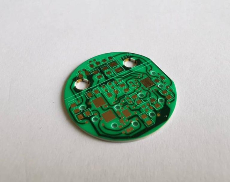
5. Prototype Implementation
5.1 Board Specifications
- Dimensions: 25mm × 15mm (excluding sensors)
- Layers: 4
- Material: FR-4
- Minimum trace/space: 4mil/4mil
- Finish: ENIG (Electroless Nickel Immersion Gold)
5.2 Component Selection
Key components include:
- Microcontroller: Nordic nRF52832 (BLE SoC)
- AFE: Maxim MAX30102 (integrated PPG sensor)
- Accelerometer: ST LIS2DH (motion compensation)
- Power Management: TI BQ51050 (wireless charging)
5.3 Firmware Architecture
The embedded software features:
- Real-time operating system (FreeRTOS)
- BLE stack with custom GATT profile
- DSP libraries for signal processing
- Power management routines
6. Performance Evaluation
Laboratory testing demonstrated:
- Heart rate accuracy: ±2 BPM during moderate exercise
- Battery life: 7 days typical usage
- Wireless range: 10m (open space)
- Motion tolerance: Reliable up to 8km/h running
7. Applications
The designed PCB enables various fitness applications:
- Real-time workout intensity monitoring
- Recovery tracking
- Sleep quality assessment
- Overtraining prevention
- Personalized exercise prescription
8. Future Enhancements
Potential improvements include:
- Integration with additional biometric sensors
- Advanced machine learning algorithms
- Solar charging capability
- Smaller form factor
9. Conclusion
This paper presented a complete design for an exercise-oriented heart rate monitoring PCB. The design addresses key challenges in wearable PPG systems, including motion artifacts, power efficiency, and signal integrity. The implemented prototype demonstrates satisfactory performance for fitness tracking applications, with potential for further refinement and commercialization.