Detailed explanation of 2 layer flexible pcb stackup design
Introduction
As electronic devices develop towards thinness and flexibility, the application of flexible printed circuit boards (FPCBs) is becoming more and more widespread. As the most basic structure of FPCB, 2-layer flexible PCBs are widely used in consumer electronics, medical equipment, automotive electronics and other fields due to their simple design and low cost. This article will discuss the stackup design of 2-layer flexible PCBs in detail, including material selection, structural design, electrical performance optimization and manufacturing process.
1. Basic structure of 2-layer flexible PCBs
2-layer flexible PCBs consist of two conductive layers (usually copper foil) and one or more insulating substrates (usually polyimide). Its basic structure is as follows:
- Top Conductor Layer: Usually copper foil, used for wiring and connecting electronic components.
- Dielectric Layer: Usually polyimide (PI), with good flexibility and high temperature resistance.
- Bottom Conductor Layer: Similar to the top conductive layer, it is used for wiring and connecting electronic components.
In some designs, a coverlay is added to the outside of the conductive layer to protect the circuit and provide additional insulation.
2. Material Selection
2.1 Conductive Layer Material
The conductive layer is usually made of copper foil because of its good conductivity and processability. Common types of copper foil are:
- Electrodeposited Copper (ED Copper): Low cost, suitable for most applications.
- Rolled Annealed Copper (RA Copper): Has better flexibility and ductility, suitable for applications that require frequent bending.
2.2 Insulating Substrate Material
The insulating substrate is usually made of polyimide (PI) because of its advantages:
- High heat resistance: Can work in high temperature environments.
- Good mechanical properties: Has high tensile strength and flexibility.
- Excellent electrical properties: low dielectric constant and low dissipation factor.
2.3 Covering layer material
The covering layer is usually made of polyimide film or photoimageable coverlay (PIC), which is used to protect the circuit and provide additional insulation.
3. Stacking design
3.1 Stacking structure
The stacking structure of a 2-layer flexible PCB is usually:
- Top Coverlay: Optional, used to protect the top conductive layer.
- Top Conductor Layer: Used for wiring and connecting electronic components.
- Dielectric Layer: Provides electrical insulation and mechanical support.
- Bottom Conductor Layer: Used for wiring and connecting electronic components.
- Bottom Coverlay: Optional, used to protect the bottom conductive layer.
3.2 Thickness Control
The thickness of a 2-layer flexible PCB is usually between 0.1mm and 0.3mm, depending on the application requirements. The key to thickness control is:
- Copper foil thickness: Common copper foil thicknesses are 1/3 oz (12μm), 1/2 oz (18μm) and 1 oz (35μm).
- Insulation substrate thickness: Common polyimide thicknesses are 12.5μm, 25μm and 50μm.
- Cover thickness: Common cover thicknesses are 25μm and 50μm.
3.3 Electrical performance optimization
The electrical performance optimization of a 2-layer flexible PCB mainly includes:
- Impedance control: Control the impedance of the transmission line by adjusting the line width, line spacing and insulation substrate thickness.
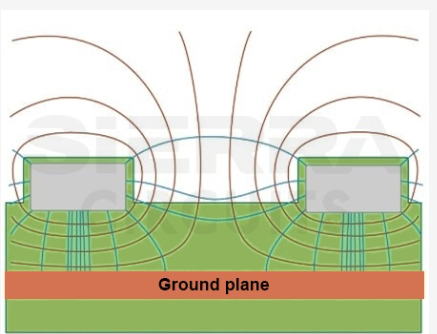
- Signal integrity: Reduce signal reflection and crosstalk through reasonable wiring design and grounding strategy.
- Power integrity: Reduce power supply noise and voltage drop through reasonable power distribution network design.
4. Manufacturing Process
4.1 Material Preparation
The first step in manufacturing a 2-layer flexible PCB is to prepare the materials, including copper foil, polyimide substrate, and cover layer.
4.2 Graphic Transfer
Graphic transfer is the process of transferring the designed circuit pattern to the copper foil, usually using photolithography or laser direct imaging (LDI) technology.
4.3 Etching
Etching is the process of removing the unwanted copper foil to form a circuit pattern. Commonly used etching solutions are ferric chloride and ammonia.
4.4 Lamination
Lamination is the process of combining the conductive layer and the insulating substrate together through a hot pressing process. The temperature, pressure, and time need to be controlled during the lamination process to ensure the bonding strength between the layers.
4.5 Drilling
Drilling is the process of forming through holes (Via) and mounting holes on the PCB. Commonly used drilling techniques are mechanical drilling and laser drilling.
4.6 Electroplating
Electroplating is the process of forming a conductive layer on the through-hole and surface, usually using chemical copper plating or electroplating copper process.
4.7 Covering layer bonding
Covering layer bonding is the process of bonding the cover layer to the conductive layer through a hot pressing process to protect the circuit and provide additional insulation.
4.8 Surface treatment
Surface treatment is the process of forming a protective layer on the surface of the PCB. Common surface treatment processes include gold plating, tin plating and OSP (organic solderability preservative).
4.9 Testing and Inspection
After manufacturing, 2-layer flexible PCBs need to be electrically tested and visually inspected to ensure that they meet design requirements and quality standards.
5. Application Cases
5.1 Consumer Electronics
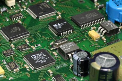
2-layer flexible PCBs are widely used in smartphones, tablets and wearable devices to connect components such as displays, cameras and sensors.
5.2 Medical Equipment
In medical equipment, 2-layer flexible PCBs are used to connect various sensors and controllers, such as electrocardiographs, blood pressure monitors, and blood glucose meters.
5.3 Automotive Electronics
In automotive electronics, 2-layer flexible PCBs are used to connect vehicle displays, sensors, and control modules, such as reversing radars, vehicle navigation, and autonomous driving systems.
6. Summary
2-layer flexible PCBs are widely used in electronic devices due to their simple design and low cost. Through reasonable material selection, stacking design, and manufacturing processes, their electrical and mechanical properties can be optimized to meet the needs of different application scenarios. With the continuous development and innovation of electronic equipment, 2-layer flexible PCBs will continue to play an important role in promoting the electronics industry to be thinner and more flexible.