Detailed explanation of EMC design principles for high-speed PCBs
This article mainly introduces the EMC design principles for high-speed PCBs. First, it introduces the basic EMC knowledge of PCB design, then explains the importance of EMC design in PCB and related items of EMC design in PCB, and finally introduces in detail the 47 principles of EMC design for high-speed PCBs. Let’s follow the editor to learn more about it.
Basic knowledge of EMC for PCB design
Some basic knowledge of electromagnetic compatibility is what excellent PCB engineers need to understand or master, mainly as follows: electromagnetic compatibility, electromagnetic field and electromagnetic wave, high-speed circuit design, signal integrity, power integrity, digital circuit, analog circuit, high-frequency circuit principle, switching power supply, etc.
The importance of EMC design in PCB
PCB is the most worthy part of EMC technology. It is not only the part with the highest operating frequency of the equipment, but also the part with the lowest level and the most sensitive to electromagnetic interference.
In the EMC design of PCB, EMC design knowledge such as grounding design, decoupling/bypass design, and crosstalk shielding are actually included. A PCB with good EMC design can not only reduce the voltage drop generated when the common mode current flows through it, but also is an important means to reduce the loop. Therefore, a device with a good decoupling and bypass design PCB is equivalent to having a strong “physique”.
The PCB board is the most basic component of electronic products and the carrier of most electronic components. When the PCB board design of a product is completed, it can be said that the interference and anti-interference characteristics of its core circuit have basically been determined.
If you want to improve its electromagnetic compatibility characteristics, you can only “encircle and intercept” it through the filtering of the interface circuit and the shielding of the shell. This not only greatly increases the subsequent cost of the product, but also increases the complexity of the product and reduces the reliability of the product.
It can be said that a good PCB board can solve most electromagnetic interference problems. As long as the transient suppression device and the filtering circuit are appropriately added when the interface circuit is arranged, most of the anti-interference and interference problems can be solved at the same time.
Enhancing electromagnetic compatibility in PCB wiring will not bring additional costs to the final completion of the product. If, in PCB board design, product designers often only focus on increasing density, reducing occupied space, making it simple, or pursuing aesthetics and uniform layout, and ignore the impact of line layout on electromagnetic compatibility, so that a large number of signals radiate into space to form interference. Then this product will cause a lot of EMC problems.
EMC design related items in PCB
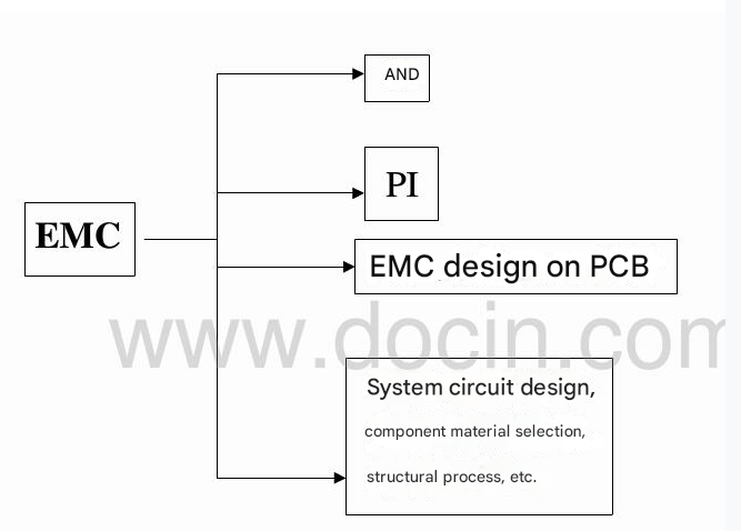
EMC design principles for high-speed PCB
Principle 1: If the PCB clock frequency exceeds 5MHZ or the signal rise time is less than 5ns, a multi-layer board design is generally required.
Reason: The signal loop area can be well controlled by using a multi-layer board design.
Principle 2: For multi-layer boards, the key wiring layer (the layer where the clock line, bus, interface signal line, RF line, reset signal line, chip select signal line and various control signal lines are located) should be adjacent to the complete ground plane, preferably between two ground planes.
Reason: Key signal lines are generally strong radiation or extremely sensitive signal lines. Wiring close to the ground plane can reduce the signal loop area, reduce its radiation intensity or improve anti-interference ability.
Principle 3: For single-layer boards, both sides of the key signal lines should be grounded;
Reason: Grounding on both sides of the key signal can reduce the signal loop area on the one hand, and prevent crosstalk between the signal line and other signal lines on the other hand.
Principle 4: For double-layer boards, a large area of ground is laid on the projection plane of the key signal line, or the ground is punched like a single-layer board.
Reason: The same as the key signal of the multi-layer board close to the ground plane
Principle 5: In a multi-layer board, the power plane should be retracted 5H-20H relative to its adjacent ground plane (H is the distance between the power and ground planes).
Reason: The retraction of the power plane relative to its return ground plane can effectively suppress edge radiation problems.
Principle 6: The projection plane of the wiring layer should be within the area of its return plane layer.
Reason: If the wiring layer is not within the projection area of the return plane layer, it will cause edge radiation problems and increase the signal loop area, thereby increasing differential mode radiation.
Principle 7: In multi-layer boards, the TOP and BOTTOM layers of a single board should not have signal lines greater than 50MHZ as much as possible.
Reason: It is best to route high-frequency signals between two plane layers to suppress their radiation to space.
Principle 8: For single boards with a board-level operating frequency greater than 50MHz, if the second layer and the second-to-last layer are wiring layers, the TOP and BOOTTOM layers should be paved with ground copper foil.
Reason: It is best to route high-frequency signals between two plane layers to suppress their radiation to space.
Principle 9: In multi-layer boards, the main working power plane of a single board (the most widely used power plane) should be adjacent to its ground plane.
Reason: The proximity of the power plane and the ground plane can effectively reduce the loop area of the power circuit.
Principle 10: In a single-layer board, there must be a ground line adjacent to and parallel to the power line.
Reason: Reduce the loop area of the power current.

Principle 11: In a double-layer board, there must be a ground line adjacent to and parallel to the power line.
Reason: Reduce the area of the power supply current loop.
Principle 12: When designing in layers, try to avoid adjacent wiring layers. If it is impossible to avoid adjacent wiring layers, the layer spacing between the two wiring layers should be appropriately increased, and the layer spacing between the wiring layer and its signal loop should be reduced.
Reason: Parallel signal traces on adjacent wiring layers will cause signal crosstalk.
Principle 13: Adjacent plane layers should avoid overlapping of their projection planes.
Reason: When the projections overlap, the coupling capacitance between layers will cause the noise between layers to couple with each other.
Principle 14: When designing PCB layout, the design principle of placing along the straight line of signal flow should be fully followed, and try to avoid back and forth.
Reason: Avoid direct coupling of signals and affect signal quality.
Principle 15: When placing multiple module circuits on the same PCB, digital circuits and analog circuits, high-speed circuits and low-speed circuits should be laid out separately.
Reason: Avoid mutual interference between digital circuits, analog circuits, high-speed circuits and low-speed circuits.
Principle 16: When there are high, medium and low speed circuits on the circuit board at the same time, the high and medium speed circuits should be kept away from the interface.
Reason: To prevent the high-frequency circuit noise from radiating outward through the interface.
Principle 17: Energy storage and high-frequency filter capacitors should be placed near unit circuits or devices with large current changes (such as power modules: input and output terminals, fans and relays).
Reason: The presence of energy storage capacitors can reduce the loop area of large current loops.
Principle 18: The filter circuit of the power input port of the circuit board should be placed close to the interface,
Reason: To prevent the line that has been filtered from being coupled again.
Principle 19: On the PCB board, the filtering, protection and isolation devices of the interface circuit should be placed close to the interface.
Reason: It can effectively achieve the effects of protection, filtering and isolation.
Principle 20: If there are both filtering and protection circuits at the interface, the principle of protection first and filtering later should be followed.
Reason: The protection circuit is used to suppress external overvoltage and overcurrent. If the protection circuit is placed after the filter circuit, the filter circuit will be damaged by overvoltage and overcurrent.
Principle 21: When laying out, ensure that the input and output lines of the filter circuit (filter), isolation and protection circuit are not coupled with each other.
Reason: When the input and output lines of the above circuits are coupled with each other, the filtering, isolation or protection effects will be weakened.
Principle 22: If an interface “clean ground” is designed on the board, the filtering and isolation devices should be placed on the isolation belt between the “clean ground” and the working ground.
Reason: Avoid mutual coupling of filtering or isolation devices through the plane layer to weaken the effect.
Principle 23: On the “clean ground”, except for filtering and protection devices, no other devices can be placed. The reason is that the purpose of the “clean ground” design is to ensure the minimum radiation of the interface, and the “clean ground” is easily coupled by external interference, so there should be no other irrelevant circuits and devices on the “clean ground”.
Principle 24: Crystals, crystal oscillators, relays, switching power supplies and other strong radiation devices should be at least 1000mil away from the single board interface connector. Reason: The interference will be radiated directly outward or coupled out of the current on the outgoing cable to radiate outward.
Principle 25: Sensitive circuits or devices (such as reset circuits, watchdog circuits, etc.) should be at least 1000mil away from the edges of the single board, especially the edges of the single board interface.
Reason: Places such as single board interfaces are the most easily coupled by external interference (such as static electricity), and sensitive circuits such as reset circuits and watchdog circuits are very likely to cause system misoperation.
Principle 26: Critical signal routing such as clocks, buses, and RF lines and other parallel routings on the same layer should meet the 3W principle.
Reason: Avoid crosstalk between signals.
Principle 27: The pads of surface-mount fuses, beads, inductors, and tantalum capacitors used in power supplies with current ≥1A should be connected to the plane layer with no less than two vias.
Reason: Reduce the equivalent impedance of vias.
Principle 28: Differential signal lines should be routed in the same layer, of equal length, and in parallel, with consistent impedance, and no other routing between differential lines.
Reason: Ensure that the common-mode impedance of the differential line pair is equal to improve its anti-interference ability.
Principle 29: Key signal routing must not cross the partition area (including the reference plane gap caused by vias and pads).
Reason: Routing across the partition area will increase the signal loop area.
Principle 30: When it is inevitable that the signal line crosses the partition of its return plane, it is recommended to use a bridge capacitor method near the signal cross-partition, and the capacitance value is 1nF.
Reason: When the signal crosses the partition, it often causes its loop area to increase. The use of the bridge ground method is to artificially set up a signal loop for it.
Principle 31: There should be no other irrelevant signal routing under the filter (filter circuit) on the single board.
Reason: Distributed capacitance will weaken the filtering effect of the filter.
Principle 32: The input and output signal lines of the filter (filter circuit) cannot be parallel or cross-routed.
Reason: Avoid direct noise coupling between the lines before and after filtering.
Principle 33: The distance between the key signal line and the edge of the reference plane is ≥3H (H is the height of the line from the reference plane).
Reason: Suppress edge radiation effect.
Principle 34: For metal shell grounding components, grounding copper should be laid on the top layer of its projection area.
Reason: The distributed capacitance between the metal shell and the grounding copper is used to suppress its external radiation and improve anti-interference.
Principle 35: In single-layer or double-layer boards, attention should be paid to the “minimization of loop area” design when wiring.
Reason: The smaller the loop area, the smaller the external radiation of the loop, and the stronger the anti-interference ability.
Principle 36: When the signal line (especially the key signal line) changes layers, the ground via should be designed near the layer change via.
Reason: It can reduce the signal loop area.
Principle 37: Clock line, bus, RF line, etc.: Strong radiation signal lines should be kept away from interface outgoing signal lines.
Reason: Avoid interference on strong radiation signal lines from coupling to outgoing signal lines and radiating outward.
Principle 38: Sensitive signal lines such as reset signal lines, chip select signal lines, system control signals, etc. should be kept away from interface outgoing signal lines.
Reason: Interface outgoing signal lines often bring in external interference, which will cause system misoperation when coupled to sensitive signal lines.
Principle 39: In single-sided and double-sided boards, the routing of filter capacitors should be filtered by filter capacitors before being sent to device pins.
Reason: Make the power supply voltage filtered before supplying power to the IC, and the noise fed back to the power supply by the IC will also be filtered out by the capacitors first.
Principle 40: In single-sided or double-sided boards, if the power supply line is very long, decoupling capacitors should be added to the ground every 3000mil, and the capacitance value should be 10uF + 1000pF.
Reason: Filter out high-frequency noise on the power supply line.

Principle 41: The grounding wire and power supply wire of the filter capacitor should be as thick and short as possible.
Reason: The equivalent series inductance will reduce the resonant frequency of the capacitor and weaken its high-frequency filtering effect.
Principle 42: Each filter capacitor for IC filtering should be placed as close to the power supply pin of the chip as possible.
Reason: The closer the capacitor is to the pin, the smaller the high-frequency loop area, and thus the smaller the radiation.
Principle 43: For the starting series matching resistor, it should be placed close to its signal output end.
Reason: The design purpose of the starting series matching resistor is to make the output impedance of the chip output end and the impedance of the series resistor equal to the characteristic impedance of the trace. The matching resistor is placed at the end, which cannot meet the above equation.
Principle 44: PCB traces cannot have right-angle or sharp-angle traces.
Reason: Right-angle traces cause impedance discontinuity, resulting in signal emission, which in turn generates ringing or overshoot, forming strong EMI radiation.
Principle 45: Avoid the layer setting of adjacent wiring layers as much as possible. If it cannot be avoided, try to make the routing in the two wiring layers perpendicular to each other or the length of parallel routing less than 1000mil.
Reason: Reduce the crosstalk between parallel routings.
Principle 46: If the single board has an internal signal routing layer, the key signal lines such as the clock are laid in the inner layer (giving priority to the preferred routing layer).
Reason: Laying the key signals in the internal routing layer can play a shielding role.
Principle 47: It is recommended to wrap the ground wire on both sides of the clock line, and the ground vias are drilled every 3000mil.
Reason: Ensure that the potential of each point on the ground wire is equal.


