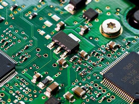
Detailed explanation of EMI avoidance techniques in PCB multilayer design
There are many ways to solve EMI problems. Modern EMI suppression methods include: using EMI suppression coatings, selecting appropriate EMI suppression components and EMI simulation design. This article starts from the most basic PCB layout and discusses the role and design techniques of PCB layering in controlling EMI radiation.
Power bus
Reasonably placing capacitors of appropriate capacity near the power pins of the IC can make the IC output voltage jump faster. Due to the limited frequency response characteristics of the capacitor, it is impossible for the capacitor to generate the harmonic power required to drive the IC output cleanly over the full frequency band. In addition, the transient voltage formed on the power bus will form a voltage drop across the inductor of the decoupling path. These transient voltages are the main source of common-mode EMI interference.
As far as the IC on the circuit board is concerned, the power layer around the IC can be regarded as an excellent high-frequency capacitor, which can collect the energy leaked by the discrete capacitor that provides high-frequency energy for clean output. In addition, the inductance of an excellent power layer should be small, so that the transient signal synthesized by the inductor is also small, thereby reducing common-mode EMI.
The connection from the power layer to the IC power pin must be as short as possible, because the rising edge of the digital signal is getting faster and faster, and it is best to connect directly to the pad where the IC power pin is located.
In order to control common-mode EMI, the power layer should help decoupling and have a sufficiently low inductance.
This power layer must be a pair of well-designed power layers. So, what is considered good? The answer depends on the layering of the power supply, the material between the layers, and the operating frequency (i.e., the function of the IC rise time). Usually, the spacing of the power layer is 6mil, and the interlayer is FR4 material, then the equivalent capacitance of the power layer per square inch is about 75pF. Obviously, the smaller the layer spacing, the greater the capacitance.
According to the current development speed of IC, devices with a rise time range of 100 to 300ps will occupy a high proportion.
For circuits with a rise time of 100 to 300ps, a 3mil layer spacing will no longer be applicable to most applications. At that time, it is necessary to adopt a layering technology with a layer spacing less than 1mil and replace the FR4 dielectric material with a material with a very high dielectric constant. Now, ceramics and ceramic plastics can meet the design requirements of circuits with a rise time of 100 to 300ps.
For today’s common 1 to 3ns rise time circuits, 3 to 6mil layer spacing and FR4 dielectric materials, high-end harmonics can usually be handled and transient signals can be kept low enough, that is, common-mode EMI can be reduced very low. The PCB layer stacking design example given in this article will assume that the layer spacing is 3 to 6mil.
Electromagnetic shielding
From the perspective of signal routing, a good layering strategy should be to put all signal routing on one or several layers, which are close to the power layer or ground layer. For power supply, a good layering strategy should be that the power layer is adjacent to the ground layer, and the distance between the power layer and the ground layer is as small as possible.
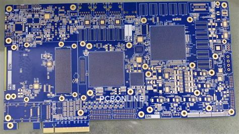
PCB stacking
What kind of stacking strategy helps shield and suppress EMI? The following layer stacking scheme assumes that the power current flows on a single layer, and a single voltage or multiple voltages are distributed in different parts of the same layer.
4-layer board
There are several potential problems with the 4-layer board design.
First, for a traditional 62mil thick four-layer board, even if the signal layer is on the outer layer and the power and ground layers are on the inner layer, the spacing between the power layer and the ground layer is still too large.
If cost is the top priority, consider the following two alternatives to the traditional 4-layer board.
Both solutions can improve EMI suppression performance, but are only applicable when the component density on the board is low enough and there is enough area around the components (to place the required power copper layer).
The first is the preferred solution, where the outer layers of the PCB are all ground layers, and the middle two layers are signal/power layers.
The power supply on the signal layer is routed with wide lines, which can make the path impedance of the power supply current low and the impedance of the signal microstrip path low. From the perspective of EMI control, this is the best 4-layer PCB structure available.
The second solution uses power and ground on the outer layers and signals on the middle two layers.
This solution is less improved than the traditional 4-layer board, and the inter-layer impedance is as poor as the traditional 4-layer board.
If the trace impedance is to be controlled, the above stacking solutions must be very careful to arrange the traces under the power and ground copper islands. In addition, the copper islands on the power or ground layers should be interconnected as much as possible to ensure DC and low-frequency connectivity.
6-layer board
If the density of components on a 4-layer board is relatively high, it is best to use a 6-layer board.
However, some stacking schemes in the 6-layer board design do not have a good enough shielding effect on the electromagnetic field and have little effect on reducing the transient signal of the power bus. Two examples are discussed below:
In the first example, the power supply and ground are placed on the 2nd and 5th layers respectively.
Due to the high impedance of the power copper, it is very unfavorable to control common-mode EMI radiation. However, from the perspective of signal impedance control, this method is very correct.
In the second example, the power supply and ground are placed on the 3rd and 4th layers respectively.
This design solves the problem of power copper impedance. Due to the poor electromagnetic shielding performance of the 1st and 6th layers, differential mode EMI increases. If the number of signal lines on the two outer layers is the least and the routing length is very short (shorter than 1/20 of the wavelength of the highest harmonic of the signal), this design can solve the differential mode EMI problem. Filling the component-free and routing-free areas on the outer layer with copper and grounding the copper area (at intervals of every 1/20 wavelength) will suppress differential mode EMI particularly well. As mentioned above, the copper area should be connected to the internal ground layer at multiple points.
General high-performance 6-layer board design generally uses the 1st and 6th layers as ground layers, and the 3rd and 4th layers for power and ground. Since there are two layers of dual microstrip signal lines in the middle between the power layer and the ground layer, the EMI suppression capability is excellent. The disadvantage of this design is that there are only two routing layers. As mentioned earlier, if the outer layer routing is short and copper is placed in the non-routing area, the same stacking can be achieved with a traditional 6-layer board.
Another 6-layer board layout is signal, ground, signal, power, ground, signal, which can achieve the environment required for advanced signal integrity design. The signal layer is adjacent to the ground layer, and the power layer and the ground layer are paired. Obviously, the disadvantage is that the stacking of the layers is unbalanced.
This usually brings trouble to processing and manufacturing.
The solution to the problem is to fill all the blank areas of the 3rd layer with copper. After copper filling, if the copper density of the 3rd layer is close to that of the power layer or the ground layer, this board can be loosely regarded as a structurally balanced circuit board. The copper-filled area must be connected to the power supply or ground. The distance between the connecting vias is still 1/20 wavelength. It is not necessary to connect everywhere, but ideally it should be connected.
10-layer board
Since the insulation isolation layer between multi-layer boards is very thin, the impedance between layers of 10 or 12-layer circuit boards is very low. As long as there is no problem with layering and stacking, excellent signal integrity can be expected. It is difficult to manufacture 12-layer boards with a thickness of 62mil, and there are not many manufacturers who can process 12-layer boards.
Since there is always an insulation layer between the signal layer and the loop layer, it is not the best to allocate the middle 6 layers to route the signal line in the 10-layer board design. In addition, it is important to make the signal layer adjacent to the loop layer, that is, the board layout is signal, ground, signal, signal, power, ground, signal, signal, ground, signal.
This design provides a good path for signal current and its loop current. The appropriate wiring strategy is to route the first layer in the X direction, the third layer in the Y direction, the fourth layer in the X direction, and so on. Intuitively looking at the routing, Layer 1 and Layer 3 are a pair of layer combinations, Layer 4 and Layer 7 are a pair of layer combinations, and Layer 8 and Layer 10 are the last pair of layer combinations. When the routing direction needs to be changed, the signal line on Layer 1 should go to Layer 3 through a “via” and then change direction. In practice, this may not always be possible, but as a design concept, it should be followed as much as possible.
Similarly, when the routing direction of the signal changes, it should go from Layer 8 and Layer 10 or from Layer 4 to Layer 7 through a via.
This routing ensures the tightest coupling between the forward path and the loop of the signal. For example, if the signal is routed on Layer 1, and the loop is on Layer 2 and only on Layer 2, then even if the signal on Layer 1 is transferred to Layer 3 through a “via”, its loop is still on Layer 2, thereby maintaining the characteristics of low inductance, large capacitance, and good electromagnetic shielding performance.
What if the actual routing is not like this?
For example, if the signal line on the first layer goes to the tenth layer through a via, the loop signal has to find the ground plane from the ninth layer, and the loop current needs to find the nearest ground via (such as the ground pin of a resistor or capacitor). If such a via happens to exist nearby, you are really lucky. If there is no such nearby via, the inductance will increase, the capacitance will decrease, and EMI will definitely increase.
When the signal line must leave the current pair of wiring layers to other wiring layers through a via, a ground via should be placed next to the via so that the loop signal can smoothly return to the appropriate ground layer. For the layered combination of the fourth and seventh layers, the signal loop will return from the power layer or the ground layer (that is, the fifth or sixth layer) because the capacitive coupling between the power layer and the ground layer is good and the signal is easy to transmit.
Design of multiple power layers
If two power layers of the same voltage source need to output large currents, the circuit board should be arranged into two sets of power layers and ground layers. In this case, an insulating layer is placed between each pair of power layers and ground layers. In this way, we get the two pairs of power buses with equal impedance that we expect to divide the current equally. If the stacking of power layers causes unequal impedance, the shunt will be uneven, the transient voltage will be much larger, and EMI will increase dramatically.
If there are multiple power supply voltages with different values on the circuit board, multiple power supply layers are required accordingly. Remember to create paired power and ground layers for different power supplies. In the above two cases, when determining the location of the paired power and ground layers on the circuit board, keep in mind the manufacturer’s requirements for balanced structures.

Summary
In circuit board design, thickness, via process and number of circuit board layers are not the key to solving the problem. Excellent layered stacking is the key to ensure bypassing and decoupling of power buses, minimizing transient voltages on power or ground layers, and shielding electromagnetic fields of signals and power supplies. Ideally, there should be an insulating isolation layer between the signal routing layer and its loop ground layer, and the paired layer spacing (or more than one pair) should be as small as possible. Based on these basic concepts and principles, a circuit board that always meets the design requirements can be designed.