Development and Application of EDA Technology
1 Introduction
Human society has entered a highly developed information society, and the development of the information society is inseparable from the progress of electronic products. While the performance of modern electronic products has improved and the complexity has increased, the price has been on a downward trend, and the pace of product replacement has also been getting faster and faster. The main factors for achieving this progress are the development of production and manufacturing technology and electronic design technology. The former is represented by micro-machining technology, which has now progressed to the deep submicron stage and can integrate tens of millions of transistors on a chip of a few square centimeters. The core of the latter is EDA technology. EDA refers to a general electronic CAD software package developed by integrating the latest achievements of electronic technology, computer technology, and intelligent technology with computers as the working platform. It can mainly assist in three aspects of design work: IC design, electronic circuit design, and PCB design. Without the support of EDA technology, it is unimaginable to complete the design and manufacture of the above-mentioned ultra-large-scale integrated circuits. Conversely, the continuous advancement of production and manufacturing technology will inevitably put forward new requirements for EDA technology.
2 Development of EDA Technology
Looking back on the development of electronic design technology in the past 30 years, EDA technology can be divided into three stages.
The 1970s was the CAD stage. People began to use computers to assist in IC layout editing and PCB layout and wiring, replacing manual operations, and the concept of computer-aided design was born.
The 1980s was the CAE stage. Compared with CAD, in addition to pure graphics drawing functions, circuit function design and structural design were added, and the two were combined through electrical connection network tables to achieve engineering design. This is the concept of computer-aided engineering. The main functions of CAE are: schematic input, logic simulation, circuit analysis, automatic layout and wiring, and PCB post-analysis.
The 1990s was the ESDA stage. Although CAD/CAE technology has achieved great success, it has not completely liberated people from the heavy design work. In the entire design process, the degree of automation and intelligence is not high. The interfaces of various EDA software vary greatly, making it difficult to learn and use, and they are incompatible with each other, which directly affects the connection between design links. Based on the above shortcomings, people began to pursue: implementing the automation of the entire design process, which is ESDA, or electronic system design automation.
3 Basic characteristics of ESDA technology
ESDA represents the latest development direction of electronic design technology today. Its basic characteristics are: designers design the scheme and divide the functions of the entire system according to the “top-down” design method. The key circuits of the system are implemented with one or several application-specific integrated circuits (ASICs), and then the system behavior level design is completed using hardware description language (HDL). Finally, the final target device is generated through synthesizers and adapters. This design method is called a high-level electronic design method. For the specific process, see Section 4.2. The following introduces several concepts related to the basic characteristics of ESDA.
3.1 “Top-down” design method
Ten years ago, the basic idea of electronic design was to select standard integrated circuits to construct a new system “bottom-up”. This design method is like building a pyramid brick by brick, which is not only inefficient, costly, but also prone to errors.
High-level design provides us with a new “top-down” design method. This design method starts with system design and divides the functional block diagram and designs the structure at the top level. Simulate and correct errors at the block diagram level, and use hardware description language to describe the high-level system behavior and verify at the system level. Then use the comprehensive optimization tool to generate a netlist of specific gate circuits, and the corresponding physical implementation level can be a printed circuit board or a dedicated integrated circuit. Since the main simulation and debugging process of the design is completed at a high level, it is conducive to early discovery of structural design errors and avoid waste of design work. At the same time, it also reduces the workload of logic function simulation and improves the first-time success rate of the design.
3.2 ASIC Design
The complexity of modern electronic products is increasing day by day. An electronic system may be composed of tens of thousands of small and medium-scale integrated circuits, which brings about the problems of large size, high power consumption and poor reliability. The effective way to solve this problem is to use ASIC (Application Specific Integrated Circuits) chips for design. ASIC can be divided into: full-custom ASIC, semi-custom ASIC, and programmable ASIC (also known as programmable logic device) according to different design methods.
When designing a full-custom ASIC chip, the designer must define the geometry and process rules of all transistors on the chip, and finally hand over the design results to the IC manufacturer for mask manufacturing. The advantage is that the chip can obtain the best performance, that is, high area utilization, fast speed and low power consumption. The disadvantages are: long development cycle, high cost, and only suitable for mass product development.
The layout design methods of semi-custom ASIC chips are different, divided into gate array design method and standard cell design method. Both methods are constrained design methods. Their main purpose is to simplify the design and shorten the development time at the expense of chip performance.
The difference between programmable logic chips and the above-mentioned mask ASICs is that after the designers complete the layout design, they can burn their own chips in the laboratory without the participation of IC manufacturers, which greatly shortens the development cycle.
Since the 1970s, programmable logic devices have gone through several development stages of PAL, GAL, CPLD, and FPGA. Among them, CPLD/FPGA is a high-density programmable logic device with an integration level of up to 2 million gates/chip. It combines the advantages of high integration of mask ASIC and the convenient design and production of programmable logic devices. It is particularly suitable for sample development or small-batch product development, so that the product can be launched at the fastest speed. When the market expands, it can be easily transferred to mask ASIC, so the development risk is greatly reduced.
The above-mentioned ASIC chips, especially CPLD/FPGA devices, have become the implementation carriers of modern high-level electronic design methods.
3.3 Hardware Description Language
Hardware Description Language (HDL) is a computer language used to design hardware electronic systems. It uses software programming to describe the logical functions, circuit structures and connection forms of electronic systems. Compared with the traditional gate-level description method, it is more suitable for the design of large-scale systems. For example, a 32-bit adder requires 500 to 1000 gates to be input using graphical input software, while using VHDL language only requires writing one line A=B+C. In addition, VHDL language is highly readable and easy to modify and find errors. Early hardware description languages, such as ABEL-HDL and AHDL, were developed by different EDA manufacturers, are incompatible with each other, and do not support multi-level design. The translation between levels must be done manually. In order to overcome the above shortcomings, the U.S. Department of Defense officially launched the VHDL (Very High Speed IC Hardware Description Language) language in 1985. In 1987, IEEE adopted VHDL as the hardware description language standard (IEEE STD-1076).
VHDL is a comprehensive hardware description language, including multiple design levels such as system behavior level, register transfer level and logic gate level, and supports mixed description of structure, data flow and behavior. Therefore, VHDL almost covers the functions of various hardware description languages in the past. The entire top-down or bottom-up circuit design process can be completed with VHDL. VHDL also has the following advantages:
(1) VHDL’s wide range of description capabilities makes it the core of high-level design, raising the focus of designers’ work to the realization and debugging of system functions, while spending less energy on physical implementation.
(2) VHDL can use concise and clear code descriptions to design complex control logic, which is flexible and convenient, and also facilitates the communication, storage and reuse of design results.
(3) VHDL design does not depend on specific devices, which facilitates process conversion.
(4) VHDL is a standard language supported by many EDA vendors, so it has good portability.
3.4 System Framework
EDA system framework is a set of specifications for configuring and using EDA software packages. Currently, major EDA systems have established frameworks, such as Cadence’s Design Framework and Mentor’s Falcon Framework, and these frameworks all comply with the unified technical standards established by the international CFI organization (CAD Framework Initiative). The Framework can optimize the combination of tool software from different EDA vendors and integrate them into an easy-to-manage unified environment. It also supports the transmission and sharing of information between tasks, between designers, and throughout the product development process. It is the basis for the implementation of concurrent engineering and top-down design methods.
4 Basic Design Methods of EDA Technology
Every advancement in EDA technology has caused a leap in the design level, which can be illustrated by Figure 1
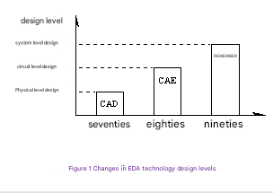
Physical level design mainly refers to IC layout design, which is generally completed by semiconductor manufacturers and is not of much significance to electronic engineers. Therefore, this article focuses on circuit level design and system level design.
4.1 Circuit-level design
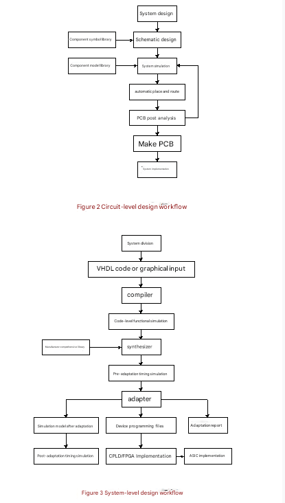
The circuit-level design workflow is shown in Figure 2. After accepting the system design task, the electronic engineer first determines the design scheme, and at the same time selects the appropriate components that can implement the scheme, and then designs the circuit schematic diagram based on the specific components. Then the first simulation is carried out, including logic simulation and fault analysis of digital circuits, AC/DC analysis and transient analysis of analog circuits. When the system is simulating, it must be supported by the component model library. The input and output waveforms simulated on the computer replace the signal source and oscilloscope in the actual circuit debugging. This simulation is mainly to verify the functional correctness of the design scheme.
After the simulation is passed, the PCB board is automatically laid out and wired according to the electrical connection network table generated by the schematic diagram. Before making the PCB board, post-analysis can also be carried out, including thermal analysis, noise and crosstalk analysis, electromagnetic compatibility analysis, reliability analysis, etc., and the result parameters after analysis can be back-labeled back to the circuit diagram for a second simulation, also known as post-simulation. This simulation is mainly to verify the feasibility of the PCB board in the actual working environment.
It can be seen that circuit-level EDA technology enables electronic engineers to fully understand the functional characteristics and physical characteristics of the system before the actual electronic system is produced, thereby eliminating development risks in the design stage, shortening development time and reducing development costs.
4.2 System-level design
Since the 1990s, the development of electronic information products has shown two obvious characteristics: one is the deepening of product complexity; the other is the urgent time limit for product launch. However, circuit-level design is essentially a single-level design based on gate-level description. All design work (including design input, simulation and analysis, design modification, etc.) is carried out at the level of basic logic gates. Obviously, this design method cannot adapt to the new situation. For this reason, a high-level electronic design method, also known as system-level design method, is introduced.
High-level design is a “concept-driven” design. Designers do not need to describe the circuit through gate-level schematics, but describe the function according to the design goal. Since they are free from the constraints of circuit details, designers can focus on creative solutions and conceptual ideas. Once these conceptual ideas are input into the computer in the form of high-level descriptions, the EDA system can automatically complete the entire design in a rule-driven manner. In this way, new concepts can be quickly and effectively turned into products, greatly shortening the product development cycle. Not only that, high-level design only defines the behavioral characteristics of the system and does not involve the implementation process. With the support of the manufacturer’s comprehensive library, the high-level description can be converted into a netlist optimized for a certain process using comprehensive optimization tools, making process conversion easy. The specific design process is shown in Figure 3.
The steps of high-level design are as follows:
Step 1:
Divide the system according to the “top-down” design method.
Step 2:
Enter VHDL code, which is the most common input method in high-level design. In addition, graphical input methods (block diagrams, state diagrams, etc.) can also be used. This input method has the advantages of being intuitive and easy to understand.
Step 3:
Compile the above design input into a standard VHDL file. For large designs, code-level functional simulation is also required, mainly to verify the correctness of the system functional design. Because for large designs, synthesis and adaptation take several hours, simulating the source code before synthesis can greatly reduce the number and time of design repetitions. Generally, this simulation step can be omitted.
Step 4:
Use the synthesizer to perform synthesis optimization on the VHDL source code and generate a netlist file of gate-level description. This is a key step in converting high-level descriptions into hardware circuits. Synthesis optimization is performed for a certain product series of ASIC chip suppliers, so the synthesis process can only be completed with the support of the corresponding manufacturer’s synthesis library. After synthesis, the generated netlist file can be used for timing simulation before adaptation. The simulation process does not involve the hardware characteristics of specific devices and is relatively rough. For general designs, this simulation step can also be omitted.
Step 5:
Use the adapter to perform logic mapping operations on the synthesized netlist file for a specific target device, including underlying device configuration, logic segmentation, logic optimization, and layout and routing. After the adaptation is completed, multiple design results are generated: ① Adaptation report, including the utilization of internal chip resources, the description of the designed Boolean equation, etc.; ② The adapted simulation model; ③ The device programming file. According to the adapted simulation model, the adapted timing simulation can be performed. Because the actual hardware characteristics of the device (such as delay characteristics) have been obtained, the simulation results can accurately predict the actual performance of the future chip. If the simulation results do not meet the design requirements, it is necessary to modify the VHDL source code or select devices with different speed qualities until the design requirements are met.
Step 6:
Load the device programming file generated by the adapter into the target chip FPGA or CPLD through a programmer or download cable. If it is a large-scale product development, it can be easily converted to ASIC form by replacing the corresponding manufacturer’s comprehensive library.
5.Conclusion
EDA technology is a revolution in the field of electronic design. It is currently in a stage of rapid development. New EDA tools are introduced every year. However, the application level of EDA technology in my country has long lagged behind that of developed countries. Therefore, the majority of electronic engineers should master this advanced technology as soon as possible. This is not only a need to improve design efficiency, but also a key factor in the development of my country’s electronic industry.The needs of the industry to survive, compete and develop in the world market.