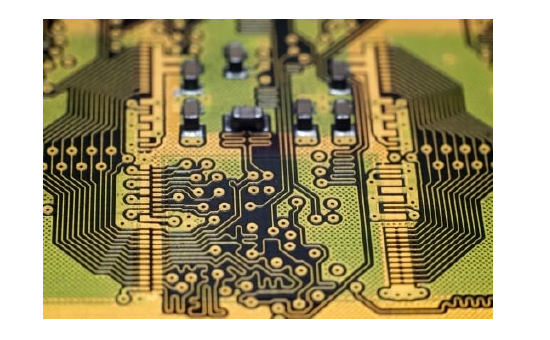
Die cavity copper metal core pcb
Benefits Of Using Copper Metal Core PCBs In Die Cavity Applications
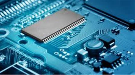
Copper metal core printed circuit boards (PCBs) have emerged as a pivotal innovation in the realm of die cavity applications, offering a multitude of benefits that enhance performance, reliability, and efficiency. These advantages stem from the intrinsic properties of copper, coupled with the sophisticated engineering of metal core PCBs, which together address the unique challenges posed by die cavity environments.
One of the foremost benefits of using copper metal core PCBs in die cavity applications is their superior thermal conductivity.
Copper, known for its excellent heat dissipation capabilities, ensures that heat generated by electronic components is efficiently transferred away from critical areas. This is particularly crucial in die cavity applications where high power densities can lead to significant thermal buildup. By mitigating heat accumulation, copper metal core PCBs help maintain optimal operating temperatures, thereby enhancing the longevity and reliability of electronic components.
In addition to thermal management, copper metal core PCBs offer enhanced mechanical stability.
The robust nature of copper provides a sturdy foundation that can withstand the mechanical stresses often encountered in die cavity applications. This durability is essential for maintaining the structural integrity of the PCB, especially in environments subject to vibrations, shocks, and other physical impacts. Consequently, the use of copper metal core PCBs contributes to the overall resilience and dependability of electronic systems.
Moreover, the electrical performance of copper metal core PCBs is another significant advantage.
Copper’s high electrical conductivity ensures minimal signal loss and efficient power distribution across the PCB. This is particularly beneficial in die cavity applications where precise and reliable signal transmission is paramount. The reduced electrical resistance offered by copper metal core PCBs translates to improved performance of the electronic components, facilitating the development of high-performance and high-reliability systems.
Furthermore, the integration of copper metal core PCBs in die cavity applications can lead to a reduction in the overall size and weight of electronic assemblies.
The efficient thermal and electrical properties of copper allow for the design of more compact and lightweight PCBs without compromising performance. This miniaturization is advantageous in applications where space constraints are a critical consideration, enabling the development of more streamlined and efficient electronic devices.
Additionally, the use of copper metal core PCBs can result in cost savings over the long term.
While the initial investment in copper-based PCBs may be higher compared to traditional materials, the enhanced durability, thermal management, and electrical performance can lead to reduced maintenance costs and longer lifespans for electronic components. This cost-effectiveness is particularly relevant in die cavity applications where reliability and longevity are paramount.
In conclusion, the benefits of using copper metal core PCBs in die cavity applications are manifold, encompassing superior thermal management, enhanced mechanical stability, improved electrical performance, and potential cost savings. These advantages make copper metal core PCBs an indispensable choice for engineers and designers seeking to optimize the performance and reliability of electronic systems in demanding environments. As technology continues to advance, the role of copper metal core PCBs in die cavity applications is likely to become even more pronounced, driving further innovations and improvements in the field.
Manufacturing Process Of Die Cavity Copper Metal Core PCBs
The manufacturing process of die cavity copper metal core PCBs is a sophisticated and intricate procedure that demands precision and expertise. This type of printed circuit board (PCB) is particularly valued for its superior thermal management capabilities, making it ideal for high-power applications. The process begins with the selection of appropriate materials, which is crucial for ensuring the final product’s performance and reliability. Typically, a metal core, often aluminum or copper, is chosen due to its excellent thermal conductivity properties.
Once the metal core is selected, the next step involves the preparation of the core material.
This includes cleaning and treating the surface to ensure it is free from contaminants that could affect the adhesion of subsequent layers. Following this, a dielectric layer is applied to the metal core. The dielectric material serves as an insulating layer, preventing electrical shorts between the conductive layers and the metal core. This layer is typically applied using a lamination process, which involves pressing the dielectric material onto the metal core under heat and pressure.
After the dielectric layer is in place, the next phase involves the application of the copper foil.
The copper foil is laminated onto the dielectric layer, forming the basis for the circuit traces. This step is critical as it determines the electrical pathways that will be etched into the board. The lamination process must be carefully controlled to ensure uniform adhesion and to prevent any air bubbles or voids that could compromise the integrity of the PCB.
Following the lamination of the copper foil, the PCB undergoes a photolithography process.
This involves coating the copper surface with a photosensitive resist material, which is then exposed to ultraviolet light through a photomask. The photomask contains the desired circuit pattern, and the UV light hardens the resist in the exposed areas. The unexposed resist is then washed away, leaving behind a pattern of resist that protects the copper during the subsequent etching process.
The etching process involves immersing the PCB in a chemical solution that dissolves the unprotected copper, leaving behind the desired circuit traces.
This step requires precise control to ensure that the etching solution does not undercut the resist-protected areas, which could lead to circuit defects. Once the etching is complete, the remaining resist is removed, revealing the copper circuit traces.
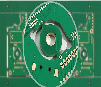
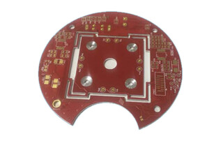
The next stage in the manufacturing process is the creation of the die cavity.
This involves milling or drilling into the metal core to create a cavity that can house electronic components. The depth and dimensions of the cavity must be precisely controlled to ensure proper fit and function of the components. This step is particularly challenging due to the hardness of the metal core, requiring specialized equipment and techniques.
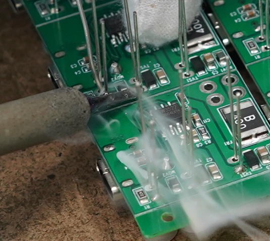
After the die cavity is created, the PCB undergoes a series of finishing processes.
These include the application of a solder mask, which protects the circuit traces from oxidation and prevents solder bridges during component assembly. Additionally, a surface finish, such as HASL (Hot Air Solder Leveling) or ENIG (Electroless Nickel Immersion Gold), is applied to the exposed copper pads to enhance solderability and protect against corrosion.
Finally, the PCB is subjected to rigorous testing to ensure it meets all electrical and mechanical specifications.
This includes electrical testing to verify continuity and isolation of the circuit traces, as well as thermal and mechanical testing to ensure the PCB can withstand the operating conditions of its intended application. Once the PCB passes all tests, it is ready for assembly and integration into electronic devices.
In conclusion, the manufacturing process of die cavity copper metal core PCBs is a complex and meticulous procedure that requires careful attention to detail at every stage. From material selection and preparation to photolithography, etching, and die cavity creation, each step is critical to ensuring the final product’s performance and reliability. Through this intricate process, manufacturers are able to produce PCBs that offer superior thermal management and are well-suited for high-power applications.
Thermal Management Advantages Of Copper Metal Core PCBs In Die Cavities
Copper metal core printed circuit boards (PCBs) have emerged as a pivotal innovation in the realm of thermal management, particularly within die cavities. The integration of copper as a core material in PCBs offers a multitude of thermal management advantages, which are crucial for the optimal performance and longevity of electronic components. As electronic devices continue to shrink in size while increasing in functionality, the need for efficient heat dissipation becomes ever more critical. Copper metal core PCBs address this need by providing superior thermal conductivity, which is essential for maintaining the integrity and performance of electronic systems.
One of the primary advantages of copper metal core PCBs in die cavities is their exceptional thermal conductivity.
Copper, as a material, boasts a thermal conductivity of approximately 400 W/mK, which is significantly higher than that of traditional PCB materials such as FR4. This high thermal conductivity allows for rapid and efficient heat transfer away from heat-generating components, thereby reducing the risk of thermal damage and ensuring stable operation. In die cavities, where space is limited and heat dissipation is paramount, the use of copper metal core PCBs can make a substantial difference in maintaining optimal temperatures.
Moreover, the enhanced thermal management capabilities of copper metal core PCBs contribute to improved reliability and longevity of electronic components.
Excessive heat can lead to thermal stress, which in turn can cause component failure, degradation of materials, and reduced performance. By effectively dissipating heat, copper metal core PCBs help to mitigate these risks, thereby extending the lifespan of electronic devices. This is particularly important in high-power applications, where the thermal load is substantial, and the consequences of overheating can be severe.
In addition to their thermal advantages, copper metal core PCBs also offer mechanical benefits that are advantageous in die cavities.
The inherent strength and durability of copper provide a robust foundation for the PCB, enhancing its structural integrity and resistance to mechanical stress. This is particularly beneficial in applications where the PCB may be subjected to physical shocks or vibrations. The combination of thermal and mechanical robustness makes copper metal core PCBs an ideal choice for demanding environments.
Furthermore, the use of copper metal core PCBs can lead to more compact and efficient designs.
The superior thermal management capabilities of copper allow for higher component densities, as the heat generated by closely packed components can be effectively dissipated. This enables the design of smaller, more powerful electronic devices without compromising on performance or reliability. In die cavities, where space is at a premium, this advantage is particularly significant.
The integration of copper metal core PCBs in die cavities also facilitates better thermal interface management.
The direct contact between the copper core and the heat-generating components ensures efficient heat transfer, reducing the thermal resistance and enhancing overall thermal performance. This is crucial in applications where precise thermal control is required to maintain the functionality and efficiency of the system.
In conclusion, the thermal management advantages of copper metal core PCBs in die cavities are manifold. Their superior thermal conductivity, enhanced reliability, mechanical robustness, and potential for compact designs make them an invaluable asset in the design and operation of modern electronic devices. As the demand for high-performance, miniaturized electronics continues to grow, the role of copper metal core PCBs in ensuring efficient thermal management will undoubtedly become increasingly important.
Design Considerations For Die Cavity Copper Metal Core PCBs
When designing die cavity copper metal core printed circuit boards (PCBs), several critical considerations must be taken into account to ensure optimal performance and reliability. These specialized PCBs are often employed in high-power applications due to their superior thermal management capabilities, which are essential for maintaining the integrity and functionality of electronic components under demanding conditions. The integration of a copper metal core within the PCB structure significantly enhances heat dissipation, thereby reducing the risk of thermal-related failures.
One of the primary design considerations is the selection of appropriate materials.
The copper core itself must be of high purity to ensure excellent thermal conductivity. Additionally, the dielectric materials used to insulate the copper core from the circuit layers must possess high thermal resistance and low thermal expansion coefficients. This ensures that the PCB can withstand the thermal stresses encountered during operation without compromising its structural integrity.
Another crucial aspect is the layout of the die cavity.
The die cavity is a recessed area within the PCB where the semiconductor die is placed. The design of this cavity must be meticulously planned to ensure proper alignment and secure placement of the die. The dimensions of the cavity should be precise, taking into account the size and shape of the die, as well as any additional components that may be housed within the cavity. Furthermore, the depth of the cavity must be carefully controlled to ensure that the die is positioned at the optimal height for effective heat transfer to the copper core.
Thermal vias are another important design element in die cavity copper metal core PCBs.
These vias are strategically placed to facilitate the efficient transfer of heat from the surface-mounted components to the copper core. The placement and density of thermal vias must be optimized to maximize heat dissipation while minimizing any potential impact on the electrical performance of the PCB. Additionally, the size and plating of these vias must be carefully considered to ensure they can handle the thermal loads without degrading over time.
Electrical performance is also a key consideration in the design of these PCBs.
The copper core, while excellent for thermal management, can introduce challenges related to signal integrity and electromagnetic interference (EMI). To mitigate these issues, careful attention must be paid to the routing of signal traces and the placement of ground planes. Shielding techniques may also be employed to protect sensitive signals from EMI. Additionally, the use of high-frequency laminates can help maintain signal integrity in high-speed applications.
Manufacturability is another critical factor in the design process.
The complexity of die cavity copper metal core PCBs requires advanced manufacturing techniques and precise control over the fabrication process. Designers must work closely with manufacturers to ensure that the PCB can be produced reliably and cost-effectively. This includes considerations such as the selection of appropriate fabrication methods, the use of advanced inspection techniques to verify the integrity of the die cavity and thermal vias, and the implementation of stringent quality control measures throughout the production process.
In conclusion, the design of die cavity copper metal core PCBs involves a careful balance of material selection, thermal management, electrical performance, and manufacturability. By addressing these considerations, designers can create PCBs that not only meet the demanding requirements of high-power applications but also deliver reliable and long-lasting performance. The integration of a copper metal core within the PCB structure offers significant advantages in terms of thermal management, making these PCBs an ideal choice for applications where heat dissipation is a critical concern.