Discussion on LED packaging structure and technology
1 Introduction
LED is a type of light-emitting device that can directly convert electrical energy into visible light and radiation energy. It has a series of characteristics such as low operating voltage, low power consumption, high luminous efficiency, extremely short luminous response time, pure light color, firm structure, impact resistance, vibration resistance, stable and reliable performance, light weight, small size, low cost, etc. It has developed by leaps and bounds and can now mass-produce high-brightness and high-performance products of various colors in the entire visible spectrum. The domestic production of red, green, orange and yellow LEDs accounts for about 12% of the world’s total. The industry goal during the “15th Five-Year Plan” period is to achieve an annual production capacity of 30 billion units, realize the large-scale production of ultra-high brightness AiGslnP LED epitaxial wafers and chips, and produce more than 1 billion red, orange and yellow ultra-high brightness LED tube cores per year, break through the key technology of GaN materials, and realize the medium-volume production of blue, green and white LEDs. It is predicted that by 2005, the international market demand for LEDs will be about 200 billion units, with sales reaching 80 billion US dollars.
In the LED industry chain, the upstream is LED substrate wafer and substrate production, the midstream industrialization is LED chip design and manufacturing, and the downstream is LED packaging and testing. The development of low thermal resistance, excellent optical properties, and high reliability packaging technology is the only way for new LEDs to become practical and marketable. In a sense, it is the link between the industry and the market. Only well-packaged products can become terminal products, be put into practical applications, and provide services to customers, making the industrial chain interlocking and seamless.
2 The particularity of LED packaging
LED packaging technology is mostly developed and evolved on the basis of discrete device packaging technology, but it has great particularity. In general, the tube core of the discrete device is sealed in the package body, and the main function of the package is to protect the tube core and complete the electrical interconnection.
LED packaging is to complete the output of electrical signals, protect the normal operation of the tube core, and output: visible light. It has both electrical parameters and optical parameter design and technical requirements. It is impossible to simply use the packaging of discrete devices for LEDs.
The core light-emitting part of the LED is a pn junction tube core composed of p-type and n-type semiconductors.
When the minority carriers injected into the pn junction recombine with the majority carriers, visible light, ultraviolet light or near-infrared light will be emitted. However, the photons emitted by the pn junction area are non-directional, that is, there is an equal probability of emission in all directions. Therefore, not all the light generated by the tube core can be released. This mainly depends on the quality of the semiconductor material, the tube core structure and geometry, the internal structure of the package and the encapsulation material. The application requires improving the internal and external quantum efficiency of the LED.
The conventional Φ5mm LED package is to bond or sinter a square tube core with a side length of 0.25mm on the lead frame.
The positive electrode of the tube core is connected to a pin through a spherical contact point and a gold wire, and the negative electrode is connected to another pin of the lead frame through a reflective cup, and then the top is encapsulated with epoxy resin. The function of the reflective cup is to collect the light emitted from the side and interface of the tube core and emit it in the desired direction angle. The epoxy resin encapsulated on the top is made into a certain shape,
which has the following functions: protecting the tube core from external erosion; using different shapes and material properties (with or without dispersion agent) to play the role of lens or diffuse lens to control the divergence angle of light; the refractive index of the tube core is too related to the refractive index of air, resulting in a very small critical angle of total reflection inside the tube core, and only a small part of the light generated by its active layer is taken out, and most of it is easily absorbed after multiple reflections inside the tube core, which is prone to total reflection and excessive light loss.
Epoxy resin with corresponding refractive index is selected as a transition to improve the light emission efficiency of the tube core.
The epoxy resin used to form the tube shell must have moisture resistance, insulation, mechanical strength, and high refractive index and transmittance of the light emitted by the tube core. When selecting packaging materials with different refractive indices, the impact of packaging geometry on photon escape efficiency is different, and the angular distribution of luminous intensity is also related to the tube core structure, light output mode, and the material and shape of the packaging lens. If a pointed resin lens is used, the light can be concentrated in the axial direction of the LED, and the corresponding viewing angle is smaller; if the top resin lens is round or flat, the corresponding viewing angle will increase.
Under normal circumstances, the wavelength of LED light changes with temperature by 0.2-0.3nm/℃, and the spectrum width increases accordingly, affecting the color vividness.
In addition, when the forward current flows through the pn junction, the heat loss causes the junction area to rise in temperature. Near room temperature, the LED’s luminous intensity will decrease by about 1% for every 1℃ increase in temperature. The package dissipates heat; it is very important to maintain color purity and luminous intensity. In the past, the method of reducing its driving current was mostly used to reduce the junction temperature. The driving current of most LEDs is limited to about 20mA. However, the light output of LEDs will increase with the increase of current. At present, the driving current of many power LEDs can reach 70mA, 100mA or even 1A. It is necessary to improve the packaging structure, a new LED packaging design concept and a low thermal resistance packaging structure and technology to improve thermal characteristics. For example, adopt a large-area chip flip-chip structure, select silver glue with good thermal conductivity, increase the surface area of the metal bracket, and directly install the silicon carrier of the solder bump on the heat sink. In addition, in the application design, the thermal design and thermal conductivity of the PCB circuit board are also very important.
After entering the 21st century, the high efficiency, ultra-high brightness, and full color of LEDs have been continuously developed.
The luminous efficiency of red and orange LEDs has reached 100Im/W, and that of green LEDs is 501m/W. The luminous flux of a single LED has also reached tens of Im. LED chips and packages no longer follow the traditional design concept and manufacturing production model. In terms of increasing the light output of the chip, research and development is not limited to changing the number of impurities in the material, lattice defects and dislocations to improve internal efficiency. At the same time, how to improve the internal structure of the tube core and package, increase the probability of photon emission inside the LED, improve light efficiency, solve heat dissipation, optimize the design of light extraction and heat sink, improve optical performance, and accelerate the surface mounting SMD process is the mainstream direction of research and development in the industry.

3 Product packaging structure types
Since the 1990s, the research and development of LED chip and material manufacturing technology has made many breakthroughs. Transparent substrate trapezoidal structure, textured surface structure, chip flip-chip structure, commercialized ultra-high brightness (above 1cd) red, orange, yellow, green, and blue LED products have been launched one after another, as shown in
Table 1. They have been used in special lighting with low and medium light flux since 2000. The upstream and midstream industries of LED have received unprecedented attention, further promoting the development of downstream packaging technology and industry. Using different packaging structure forms and sizes, tube cores with different luminous colors and their two-color or three-color combinations, a variety of series, varieties, and specifications of products can be produced.
The types of LED product packaging structures are shown in Table 2,
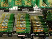
and are also classified according to the characteristics of luminous color, chip material, luminous brightness, size, etc. A single tube core generally constitutes a point light source, and multiple tube cores can generally be assembled to form a surface light source and a line light source for information, status indication and display. The light-emitting display also uses multiple tube cores, which are combined with appropriate optical structures through appropriate connection of the tube cores (including series and parallel connection) to form the light-emitting segments and light-emitting points of the light-emitting display. Surface-mounted LEDs can gradually replace pin-type LEDs, and the application design is more flexible. They have occupied a certain share in the LED display market and have an accelerating development trend. Some solid lighting sources have been launched on the market, becoming the medium- and long-term development direction of LEDs in the future.
4 Pin-type package
LED pin-type package uses lead frames as pins for various package shapes. It is the first package structure successfully developed and put on the market. There are many varieties and the technology is highly mature. The internal structure and reflective layer of the package are still being improved. Standard LEDs are considered by most customers to be the most convenient and economical solution in the current display industry. Typical traditional LEDs are placed in packages that can withstand 0.1W input power. 90% of the heat is dissipated from the negative lead frame to the PCB board and then to the air. How to reduce the temperature rise of the pn junction during operation is a must for packaging and application. The encapsulation material is mostly high-temperature curing epoxy resin, which has excellent optical properties, good process adaptability, and high product reliability. It can be made into colored transparent or colorless transparent and colored scattering or colorless scattering lens packages. Different lens shapes constitute a variety of shapes and sizes. For example, the circle is divided into several types according to the diameter, such as Φ2mm, Φ3mm, Φ4.4mm, Φ5mm, Φ7mm, etc. Different components of epoxy resin can produce different luminous effects. There are many different packaging structures for colorful point light sources: ceramic base epoxy resin packaging has good operating temperature performance, the pins can be bent into the required shape, and the volume is small; metal base plastic reflective cover packaging is an energy-saving indicator light, suitable for power indication; the flashing type combines the CMOS oscillation circuit chip with the LED tube core, which can generate flashing light with strong visual impact; the two-color type is composed of two tube cores with different luminous colors, which are packaged in the same epoxy resin lens. In addition to the two colors, a third mixed color can be obtained. It is widely used in large-screen display systems and can be packaged to form a two-color display device; the voltage type combines the constant current source chip with the LED tube core, which can directly replace various voltage indicator lights of 5-24V. The surface light source is formed by bonding multiple LED tube cores to the specified position of the micro PCB board, using a plastic reflective frame cover and potting epoxy resin. The different designs of the PCB board determine the arrangement and connection of the external leads, and there are structural forms such as dual-row in-line and single-row in-line. Hundreds of package shapes and sizes have been developed for point and surface light sources for market and customer application.
LED light-emitting displays can be composed of various multi-digit products such as digital tubes or M-shaped tubes, symbol tubes, and matrix tubes, and can be designed into various shapes and structures according to actual needs. Taking digital tubes as an example, there are three packaging structures: reflective cover type, monolithic integrated type, and single seven-segment type. There are two connection methods: common anode and common cathode. One digit is usually called a digital tube, and more than two digits are generally called displays. The reflective cover type has the characteristics of large font size, low material consumption, and flexible assembly. It is generally made of white plastic into a seven-segment shell with a reflective cavity. A single LED tube core is bonded to a PCB board that is aligned with the seven reflective cavities of the reflective cover. The center position of the bottom of each reflective cavity is the light-emitting area formed by the tube core. The leads are bonded by pressure welding, and epoxy resin is dripped into the reflective cover. It is aligned and bonded with the PCB board with the tube core, and then cured. The reflective cover type is divided into two types: empty seal and solid seal. The former uses epoxy resin with scattering agent and dye, and is mostly used for single-bit and double-bit devices; the latter is covered with color filter and uniform light film, and transparent insulating glue is applied on the tube core and the bottom plate to improve the light output efficiency. It is generally used for digital display with more than four digits. The monolithic integrated type is to make a large number of seven-segment digital display graphic tube cores on the luminous material wafer, and then cut and divide them into single-chip graphic tube cores, and bond, press weld, and package the shell with lens (commonly known as fisheye lens). The single-strip seven-segment type cuts the already made large-area LED chip into light strips containing one or more tube cores, so that the same seven strips are bonded to the digital font frame, and are formed by press welding and epoxy resin packaging. The characteristics of the monolithic type and the single-strip type are miniaturization, and dual-in-line packaging can be used. Most of them are special products. The LED light column display is placed on a 106mm long circuit board, with 101 tube cores (up to 201 tube cores). It is a high-density package. It uses the principle of optical refraction to make the point light source pass through the 13-15 gratings of the transparent cover to form an image, and complete the display of each tube core from point to line. The packaging technology is relatively complex.
The electroluminescent mechanism of the semiconductor pn junction determines that LED cannot produce white light with a continuous spectrum. At the same time, a single LED cannot produce more than two high-brightness monochromatic lights. It can only use fluorescent substances during packaging, and apply fluorescent powder on the blue or ultraviolet LED tube core to indirectly produce a broadband spectrum and synthesize white light; or use several (two or three, multiple) tube cores that emit different colors to be packaged in a component shell, and form a white light LED through the mixing of colored light. Both methods have been put into practical use. In 2000, Japan produced 100 million white light LEDs, which developed into a type of product that emits white light stably, and designed and assembled multiple white light LEDs into electric light sources that do not require high luminous flux, mainly for local decorative purposes, and pursue trendy light sources.
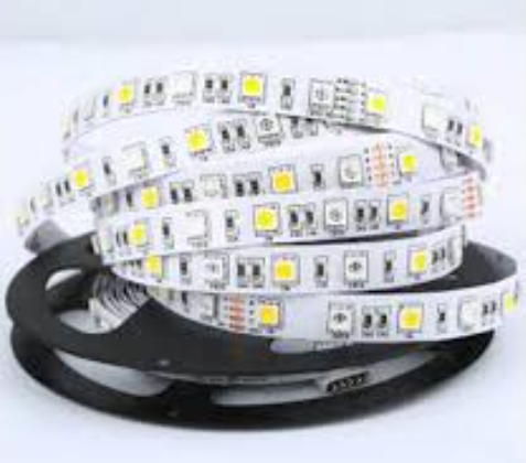
5 Surface mount package
In 2002, surface mount packaged LEDs (SMD LEDs) were gradually accepted by the market and gained a certain market share. The shift from pin-type packages to SMDs was in line with the general trend of the entire electronics industry, and many manufacturers launched such products.
Most of the early SMD LEDs used an improved SOT-23 with a transparent plastic body, with an outer size of 3.04×1.11mm and a reel-type container with braided packaging. Based on SOT-23, the SLM-125 series and SLM-245 series LEDs with high brightness SMDs with lenses were developed. The former is single-color luminescence, and the latter is two-color or three-color luminescence. In recent years, SMD LED has become a hot spot for development, which has solved the problems of brightness, viewing angle, flatness, reliability, consistency, etc. It uses lighter PCB boards and reflective layer materials, requires less epoxy resin to be filled in the display reflective layer, and removes the heavier carbon steel pins. By reducing the size and weight, the weight of the product can be easily reduced by half, and the application will be more perfect, especially suitable for indoor and semi-outdoor full-color display applications.
The soldering pad is an important channel for heat dissipation. The data of SMD LED provided by manufacturers are based on 4.0×4.0mm soldering pads. Reflow soldering can be designed to make the soldering pad equal to the pin. Ultra-high brightness LED products can use PLCC (plastic encapsulated lead chip carrier)-2 package, with an outer size of 3.0×2.8mm. The high-brightness tube core is assembled by a unique method. The product thermal resistance is 400K/W, and it can be welded in CECC mode. Its luminous intensity reaches 1250mcd at a driving current of 50mA. The character height of the seven-segment one-, two-, three- and four-digit SMD LED display devices is 5.08-12.7mm, and the display size selection range is wide. The PLCC package avoids the manual insertion and pin alignment process required for the pin seven-segment digital display, meets the production requirements of automatic pick-and-place equipment, has flexible application design space, and displays bright and clear. The multi-color PLCC package has an external reflector, which can be easily combined with a light-emitting tube or light guide, replacing the current transmissive optical design with a reflective type to provide uniform lighting for a large area, and developing a power SMD LED package that works under 3.5V, 1A driving conditions.
06 Power-type package
LED chips and packages are developing towards high power, generating luminous flux 10-20 times greater than Φ5mmLED under high current. Effective heat dissipation and non-degrading packaging materials must be used to solve the light decay problem. Therefore, the tube shell and package are also its key technologies, and LED packages that can withstand several W of power have appeared. 5W series white, green, blue-green, blue power LEDs have been supplied since early 2003. The white LED light output reaches 1871m, and the light efficiency is 44.31m/W. In order to solve the green light decay problem, we developed LEDs that can withstand 10W power, which can be used for large-scaleThe tube size is 2.5×2.5mm, it can work at 5A current, and the light output reaches 2001m, which has great development space as a solid lighting source.
Luxeon series power LED is to flip-chip solder the A1GalnN power flip-chip tube core on a silicon carrier with solder bumps, and then put the flip-chip soldered silicon carrier into the heat sink and tube shell, and bond the leads for packaging. This package is the best design for light collection efficiency, heat dissipation performance, and increased working current density. Its main features: low thermal resistance, generally only 14℃/W, only 1/10 of conventional LEDs; high reliability, the package is filled with stable flexible gel, in the range of -40-120℃, the internal stress caused by sudden temperature changes will not cause the gold wire to disconnect from the lead frame, and prevent the epoxy resin lens from yellowing, and the lead frame will not be stained by oxidation; the optimal design of the reflector cup and lens makes the radiation pattern controllable and the optical efficiency the highest. In addition, its output light power, external quantum efficiency and other performance are excellent, which brings the LED solid light source to a new level.
The packaging structure of the Norlux series power LED is a multi-chip combination with a hexagonal aluminum plate as the base (making it non-conductive). The base diameter is 31.75mm, and the light-emitting area is located in its center. The diameter is about (0.375×25.4) mm, which can accommodate 40 LED tube cores. The aluminum plate also serves as a heat sink. The bonding wires of the tube core are connected to the positive and negative electrodes through two contact points made on the base. The number of tube cores arranged on the base is determined according to the required output light power. The ultra-high brightness AlGaInN and AlGaInP tube cores that can be packaged can emit monochrome, color or synthetic white light, and finally encapsulated with high refractive index materials according to the optical design shape. This package uses conventional tube core high-density combination packaging, with high light extraction efficiency, low thermal resistance, better protection of the tube core and bonding wires, and high light output power under high current. It is also a promising LED solid light source.
In application, the packaged products can be assembled on a metal core PCB with an aluminum interlayer to form a power density LED. The PCB is used as the wiring for connecting the device electrodes, and the aluminum core interlayer can be used as a heat sink to obtain a higher luminous flux and photoelectric conversion efficiency. In addition, the packaged SMD LED is very small and can be flexibly combined to form a variety of lighting sources such as module type, light guide plate type, focusing type, and reflective type.
The thermal characteristics of power LEDs directly affect the operating temperature, luminous efficiency, luminous wavelength, and service life of LEDs. Therefore, the packaging design and manufacturing technology of power LED chips are particularly important.
7 LED development and application prospects
In recent years, the luminous efficiency of LEDs has increased by 100 times and the cost has decreased by 10 times. It is widely used in large-area full-color screens for graphic display, status indication, sign lighting, signal display, backlight source of LCD displays, automobile combination taillights and interior lighting, etc. Its development prospects have attracted major lighting manufacturers around the world to join the LED light source and market development. White light LED has great development and application prospects. It is economical and environmentally friendly when used as a solid lighting device. It is gradually replacing traditional incandescent lamps. The annual growth rate in the world is over 20%. The United States, Japan, Europe and Taiwan Province of China have all launched semiconductor lighting plans. At present, the luminous efficiency of ordinary white light LED is 251m/W. Experts predict that it may exceed 3001m/W in 2005. The excellent heat dissipation and optical properties of power LED are more suitable for the field of ordinary lighting. It is considered by academia and industry as the only way for LED to enter the lighting market. In order to replace fluorescent lamps, white light LED must have a luminous efficiency of 150-2001m/W, and the price per 1m should be significantly lower than 0.015/1m (the current price is about 0.25$/1m, and the price of red LED is 0.065/1m). There are still many technical problems to be studied to achieve this goal, but it is not a very distant thing to overcome and solve these problems. According to the principles of solid-state luminescence physics, the luminous efficiency of LED can be close to 100%. Therefore, LED is hailed as the new light source of the 21st century and is expected to become the fourth generation of light sources after incandescent lamps, fluorescent lamps, and high-intensity gas discharge lamps.
8 Conclusion
There are more than 20 upstream and midstream research and production units and more than 150 back-end packaging companies in the domestic LED industry, and high-end packaging products have not yet been launched on the market. At present, the industrialization research of GaN-based blue-green LED midstream process technology has been completed, and efforts have been made to make the performance indicators of products reach the level of similar products of the same period abroad in the short term, and strive to achieve a monthly production capacity of 10kk in a relatively short period of time, and develop new products such as power LED chips for white light sources. The Ministry of Science and Technology will invest 80 million yuan to launch the National Semiconductor Lighting Project, pay attention to terminal products, start with special products, take automobiles and urban landscape lighting as market breakthroughs, and put high-power and high-brightness LEDs in a prominent position. Its achievements will serve the Beijing Olympics and the Shanghai World Expo. There is no doubt that the substrates, epitaxy, chips, packaging and applications in the industrial chain need to develop together and be cultivated through interaction among multiple parties. Packaging is the connecting part of the industrial chain and requires attention and importance.