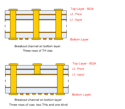
Discussion on Vias in PCB Design
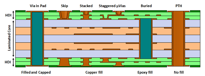
Vias are a crucial component of multilayer PCBs, and drilling costs typically account for 30% to 40% of the overall PCB fabrication cost. Simply put, every hole on a PCB can be called a via. Based on their function, vias can be categorized into two types: one for electrical connection between layers; the other for securing or positioning components. From a manufacturing process perspective, these vias are generally divided into three categories: blind vias, buried vias, and through vias. Blind vias are located on the top and bottom surfaces of a printed circuit board (PCB). They have a certain depth and connect the surface circuitry to the underlying inner layers. The depth typically does not exceed a certain ratio (hole diameter). Buried vias are connection holes located on the inner layers of a PCB and do not extend to the board’s surface. Both types of vias are located on the inner layers of the PCB and are formed using a through-hole forming process before lamination. The via formation process may also overlap several inner layers. The third type, called through vias, passes through the entire PCB and can be used for internal interconnects or as mounting holes for components. Because through-holes are easier to implement and less expensive, they are used in most printed circuit boards (PCBs) rather than the other two types of vias. Unless otherwise specified, all vias mentioned below are considered through-holes.
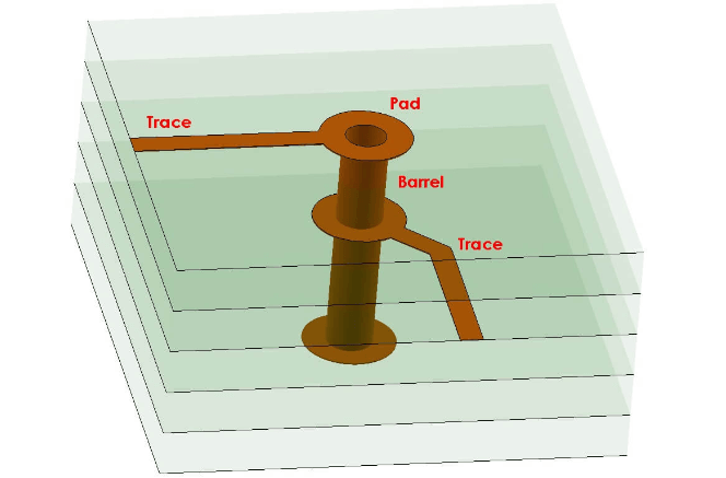
From a design perspective, a via consists of two main components: the central drill hole and the surrounding pad area, as shown in the figure below. The dimensions of these two components determine the size of the via. Obviously, in high-speed, high-density PCB designs, designers prefer to make vias as small as possible to allow for more wiring space. Furthermore, smaller vias reduce their inherent parasitic capacitance, making them more suitable for high-speed circuits. However, reducing hole size also increases cost, and via size cannot be reduced indefinitely. It is limited by process technologies such as drilling and plating. Smaller holes require longer drilling times and are more likely to deviate from the center. Furthermore, when the hole depth exceeds six times the drill diameter, uniform copper plating cannot be guaranteed on the hole walls. For example, the thickness (via depth) of a typical 6-layer PCB is currently around 50 mils, so the minimum drill diameter that PCB manufacturers can provide is only 8 mils.
1.Parasitic Capacitance of Vias
Vias inherently have parasitic capacitance to ground. If the diameter of the via isolation hole on the ground plane is D2, the diameter of the via pad is D1, the thickness of the PCB is T, and the dielectric constant of the substrate is ε, then the parasitic capacitance of the via is approximately:
C = 1.41εTD1/(D2-D1)
The primary impact of via parasitic capacitance on a circuit is that it prolongs the signal rise time, reducing circuit speed. For example, for a 50-mil-thick PCB, if a via with a 10-mil inner diameter and a 20-mil pad diameter is used, and the distance between the pad and the ground copper is 32 mils, the via’s parasitic capacitance can be approximated using the formula above: C = 1.41 x 4.4 x 0.050 x 0.020 / (0.032 – 0.020) = 0.517 pF. The rise time change caused by this capacitance is: T10 – 90 = 2.2C (Z0 / 2) = 2.2 x 0.517 x (55 / 2) = 31.28 ps. These values show that while the rise time slowing effect of a single via’s parasitic capacitance isn’t significant, designers should still carefully consider it if multiple vias are used for interlayer switching within a trace.
2.Parasitic Inductance of Vias
Similarly, vias have both parasitic capacitance and parasitic inductance. In the design of high-speed digital circuits, the parasitic inductance of vias often poses a greater threat than the parasitic capacitance. Its parasitic series inductance weakens the contribution of the bypass capacitor and reduces the filtering effectiveness of the entire power supply system. The following formula can be used to simply calculate the approximate parasitic inductance of a via:
L = 5.08h [ln(4h/d) + 1], where L is the via inductance, h is the via length, and d is the diameter of the center hole. As can be seen from the formula, the via diameter has a minor impact on the inductance, while the via length has the greatest influence. Using the above example again, the via inductance can be calculated as: L = 5.08 x 0.050 [ln(4 x 0.050/0.010) + 1] = 1.015nH. If the signal rise time is 1ns, then its equivalent impedance is: XL = πL / T10 – 90 = 3.19Ω. This impedance is not negligible when high-frequency currents are flowing. In particular, the bypass capacitor must pass through two vias when connecting the power layer and the ground layer, which multiplies the parasitic inductance of the vias.
3.Via Design in High-Speed PCBs
The above analysis of via parasitic characteristics shows that in high-speed PCB design, seemingly simple vias can often have significant negative effects on circuit design. To minimize the adverse effects of via parasitics, the following should be considered in the design:
- Consider both cost and signal quality when selecting a reasonable via size. For example, for 6-10 layer memory module PCBs, 10/20 mil (drill/pad) vias are preferred. For smaller, high-density boards, 8/18 mil vias can also be used. Current technology makes it difficult to use smaller via sizes. For vias for power or ground traces, consider using larger sizes to reduce impedance.
- The two formulas discussed above indicate that using thinner PCBs helps reduce the two parasitic parameters of vias.
- Signal traces on the PCB should avoid switching layers as much as possible, which means avoiding unnecessary vias.
- Vias should be placed near power and ground pins. The traces between the vias and the pins should be as short as possible, as these increase inductance. Power and ground traces should also be as thick as possible to reduce impedance.
- Place ground vias near signal vias that switch layers to provide the closest possible return path for the signal. You can even place a large number of redundant ground vias on the PCB. Of course, flexibility is required in design. The via model discussed above assumes pads on every layer. Sometimes, pads on certain layers can be reduced or even eliminated. Especially when the via density is very high, it may cause a broken groove to form in the copper layer, which will cut off the circuit. To solve this problem, in addition to moving the position of the via, we can also consider reducing the size of the via pad in the copper layer.