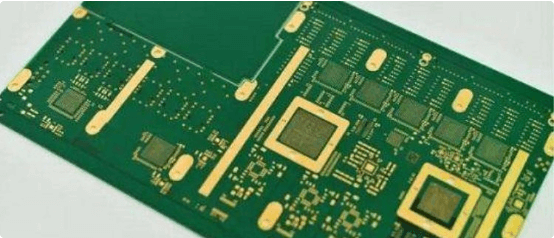
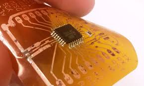
Diy flexible pcb
How To Design Your Own DIY Flexible PCB At Home
Designing your own DIY flexible PCB at home can be a rewarding and cost-effective endeavor, especially for electronics enthusiasts and hobbyists. Flexible PCBs, or flex circuits, offer unique advantages over traditional rigid PCBs, including the ability to bend and conform to various shapes, which can be particularly useful in compact or irregularly shaped electronic devices. To embark on this project, it is essential to understand the fundamental steps involved in designing and fabricating a flexible PCB.
First and foremost, it is crucial to have a clear understanding of your project requirements.
This includes defining the circuit’s functionality, the components you plan to use, and the physical constraints of your design. Once you have a clear vision, the next step is to create a schematic diagram. This diagram serves as a blueprint for your circuit, detailing the connections between various components. Software tools such as KiCad, Eagle, or Altium Designer can be invaluable in this phase, as they provide user-friendly interfaces for creating and editing schematics.
After completing the schematic, the next step is to design the PCB layout.
This involves placing the components on the board and routing the electrical connections between them. When designing a flexible PCB, it is essential to consider the mechanical properties of the material. Flexible PCBs are typically made from polyimide, a material known for its excellent flexibility and thermal stability. However, excessive bending or twisting can still cause damage, so it is important to design the layout with minimal stress points. Additionally, using curved traces instead of sharp angles can help distribute mechanical stress more evenly.
Once the layout is finalized, the next step is to generate the Gerber files.
These files are a standard format used by PCB manufacturers to fabricate the board. They contain information about the copper layers, solder mask, and silkscreen layers. It is important to double-check the Gerber files for any errors or inconsistencies before proceeding to fabrication.
For the DIY enthusiast, fabricating a flexible PCB at home can be challenging but not impossible.
One common method is to use a laser printer and a heat transfer process. Start by printing the PCB layout onto a special transfer paper using a laser printer. Next, place the transfer paper onto a sheet of polyimide and use a laminator or an iron to transfer the toner from the paper to the polyimide. After the transfer is complete, etch the board using a ferric chloride solution to remove the unwanted copper, leaving behind the desired circuit pattern.
Following the etching process, the next step is to drill any necessary holes for through-hole components. A precision drill press or a handheld rotary tool can be used for this purpose. After drilling, clean the board thoroughly to remove any residual etchant or debris.
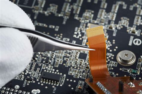
Finally, assemble the components onto the flexible PCB. This step requires careful soldering, as excessive heat can damage the flexible substrate. Using a low-temperature soldering iron and practicing good soldering techniques can help ensure a successful assembly.
In conclusion, designing and fabricating a DIY flexible PCB at home involves several meticulous steps, from schematic creation to final assembly. By understanding the unique properties of flexible materials and employing careful design and fabrication techniques, you can create custom flexible PCBs tailored to your specific project needs. This process not only enhances your technical skills but also provides a deeper appreciation for the intricacies of modern electronics design.
Essential Tools And Materials For DIY Flexible PCB Projects
Creating a DIY flexible printed circuit board (PCB) can be a rewarding endeavor for electronics enthusiasts and professionals alike. To embark on such a project, it is crucial to have a comprehensive understanding of the essential tools and materials required. This knowledge not only ensures the successful completion of the project but also enhances the quality and functionality of the final product.
First and foremost, the foundation of any flexible PCB project is the substrate material.
Polyimide is the most commonly used substrate due to its excellent thermal stability, flexibility, and electrical insulation properties. It is essential to select a high-quality polyimide film to ensure the durability and performance of the flexible PCB. Additionally, copper foil is required for the conductive traces. The thickness of the copper foil can vary depending on the specific requirements of the project, but it is typically available in thicknesses ranging from 18 to 70 micrometers.
Moving on to the tools, a reliable computer-aided design (CAD) software is indispensable for designing the PCB layout.
Software such as Eagle, KiCad, or Altium Designer allows for precise and efficient design of the circuit, ensuring that all components are correctly placed and connected. Once the design is complete, a laser printer or a photoplotter is necessary to print the design onto a transparent film or directly onto the substrate. This step is crucial for creating the mask that will guide the etching process.
The etching process itself requires a few specific materials and tools.
Ferric chloride or ammonium persulfate are commonly used etching solutions that dissolve the unwanted copper, leaving behind the desired circuit pattern. It is important to handle these chemicals with care, using appropriate safety equipment such as gloves and goggles. A plastic or glass container is needed to hold the etching solution, and a pair of plastic tweezers is useful for handling the substrate during the etching process.
After etching, the next step is to drill holes for through-hole components.
A precision drill press or a handheld rotary tool with micro drill bits is essential for this task. The drill bits should be of various sizes to accommodate different component leads. It is important to drill the holes accurately to ensure proper alignment and connectivity of the components.
Soldering is another critical step in the assembly of a flexible PCB.
A high-quality soldering iron with a fine tip is necessary for precise soldering of small components. Additionally, solder wire, flux, and a desoldering pump or wick are essential tools for this process. It is important to use lead-free solder to comply with environmental regulations and ensure the safety of the final product.
Finally, testing and troubleshooting tools are indispensable for verifying the functionality of the flexible PCB. A digital multimeter is essential for measuring voltage, current, and resistance, while an oscilloscope can be used to analyze signal waveforms. Additionally, a power supply unit is necessary to provide the required voltage and current to the circuit during testing.
In conclusion, embarking on a DIY flexible PCB project requires a thorough understanding of the essential tools and materials. From selecting the appropriate substrate and copper foil to utilizing CAD software for design, and from etching and drilling to soldering and testing, each step demands precision and care. By equipping oneself with the right tools and materials, one can ensure the successful completion of a high-quality flexible PCB that meets the desired specifications and performance standards.
Step-By-Step Guide To Etching Your DIY Flexible PCB
Creating your own flexible printed circuit board (PCB) can be a rewarding and cost-effective endeavor, especially for hobbyists and small-scale projects. The process of etching a DIY flexible PCB involves several meticulous steps, each requiring careful attention to detail to ensure a successful outcome. This guide will walk you through the essential stages of etching your flexible PCB, from preparing your materials to the final inspection.
To begin with, gather all necessary materials and tools.
You will need a flexible copper-clad substrate, a laser printer, glossy paper, ferric chloride etchant, a plastic container, a laminator or iron, acetone, and protective gear such as gloves and goggles. Ensuring you have all these items on hand before starting will streamline the process and prevent unnecessary interruptions.
The first step involves designing your PCB layout using PCB design software.
Once your design is complete, print it onto glossy paper using a laser printer. The toner from the laser printer will act as a resist during the etching process. It is crucial to print the design in mirror image to ensure it transfers correctly onto the copper-clad substrate.
Next, cut the flexible copper-clad substrate to the desired size, slightly larger than your printed design.
Clean the copper surface thoroughly with acetone to remove any oils or contaminants that could interfere with the toner transfer. After cleaning, position the printed design face down onto the copper surface.
Using a laminator or an iron set to a medium-high temperature, apply heat and pressure to transfer the toner from the glossy paper to the copper.
This step requires patience and precision; ensure even heat distribution and avoid moving the paper to prevent smudging. After sufficient heating, allow the board to cool before carefully peeling off the paper, leaving the toner design adhered to the copper.
With the toner design now on the copper-clad substrate, the next phase is etching.
Prepare a ferric chloride solution in a plastic container, following the manufacturer’s instructions for concentration and safety precautions. Submerge the board in the etchant, agitating gently to ensure even exposure. The ferric chloride will dissolve the exposed copper, leaving only the areas protected by the toner.
Monitor the etching process closely, as over-etching can damage the fine details of your design.
Once the unwanted copper is fully dissolved, remove the board from the etchant and rinse it thoroughly with water to stop the chemical reaction. Dispose of the used ferric chloride solution responsibly, adhering to local environmental regulations.
After etching, the next step is to remove the toner resist.
Use acetone and a soft cloth to gently wipe away the toner, revealing the copper traces of your PCB design. Inspect the board carefully for any defects or incomplete etching. If necessary, use a fine-tipped tool to correct minor imperfections.
Finally, to enhance the durability and performance of your flexible PCB, consider applying a protective coating such as solder mask or conformal coating. This will protect the copper traces from oxidation and mechanical wear. Once the protective coating is applied and cured, your DIY flexible PCB is ready for use.
In conclusion, etching your own flexible PCB requires a methodical approach and attention to detail. By following these steps and taking appropriate safety measures, you can create high-quality, custom PCBs tailored to your specific needs. This hands-on process not only provides a deeper understanding of PCB fabrication but also offers the satisfaction of crafting a functional electronic component from start to finish.
Common Mistakes To Avoid When Creating DIY Flexible PCBs
Creating DIY flexible PCBs can be an exciting and rewarding endeavor, offering the opportunity to design custom electronic circuits that are both versatile and compact. However, the process is fraught with potential pitfalls that can compromise the functionality and reliability of the final product. To ensure success, it is crucial to be aware of common mistakes and take steps to avoid them.
One of the most frequent errors in DIY flexible PCB creation is inadequate planning and design.
Many hobbyists rush into the fabrication process without thoroughly considering the layout and requirements of their circuit. This can lead to issues such as improper component placement, insufficient trace widths, and inadequate spacing between traces, all of which can result in electrical shorts or signal interference. To mitigate these risks, it is essential to use PCB design software to meticulously plan the layout, ensuring that all components are correctly positioned and that traces are appropriately sized and spaced.
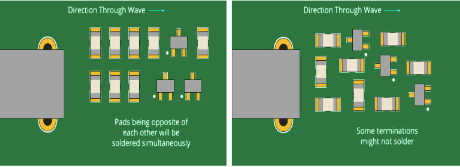
Another common mistake is neglecting to account for the mechanical properties of flexible PCBs.
Unlike rigid PCBs, flexible PCBs must endure bending and flexing, which can place significant stress on the traces and solder joints. Failing to design for these mechanical stresses can lead to cracked traces and broken connections. To avoid this, it is important to use curved traces instead of sharp angles, as well as to incorporate strain relief features such as fillets and teardrops at trace junctions. Additionally, selecting materials with appropriate flexibility and durability is crucial to ensure the longevity of the PCB.
The choice of materials is another area where DIY enthusiasts often falter.
Using inappropriate or substandard materials can severely impact the performance and reliability of the flexible PCB. For instance, using a substrate that is not designed for flexibility can result in cracking and delamination. It is vital to select high-quality, flexible substrates such as polyimide or polyester, which are specifically engineered for use in flexible PCBs. Furthermore, choosing the right type of adhesive and protective coatings is essential to prevent moisture ingress and environmental damage.
Soldering is another critical aspect where mistakes are commonly made.
Improper soldering techniques can lead to weak joints, which are prone to failure under mechanical stress. It is important to use a soldering iron with precise temperature control to avoid overheating the components and the flexible substrate. Additionally, using the correct type of solder and flux is essential to ensure strong, reliable joints. Practicing good soldering techniques, such as using the right amount of solder and ensuring proper wetting of the joint, can significantly enhance the durability of the connections.
Lastly, testing and quality control are often overlooked in DIY flexible PCB projects.
Skipping these crucial steps can result in undetected defects that compromise the functionality of the final product. It is important to thoroughly test the PCB for continuity, shorts, and proper operation before integrating it into the final application. Using tools such as multimeters, oscilloscopes, and specialized PCB testing equipment can help identify and rectify issues early in the process.
In conclusion, creating DIY flexible PCBs requires careful planning, attention to detail, and adherence to best practices. By avoiding common mistakes such as inadequate design, improper material selection, poor soldering techniques, and neglecting testing, hobbyists can significantly improve the chances of producing a functional and reliable flexible PCB. Taking the time to understand and address these potential pitfalls will ultimately lead to more successful and satisfying DIY electronics projects.