Do you know how to do wiring? Do you know how to break through the bottleneck of wiring level?
Do you know how to break through the bottleneck of wiring level? For PCB engineers, wiring is not only an important link that consumes time and effort, but also a link that tests the true technical level of PCB engineers. If you want to make a good PCB board, wiring work is a basic link that cannot be ignored. So, how to break through the bottleneck of wiring level and make PCB wiring more perfect?
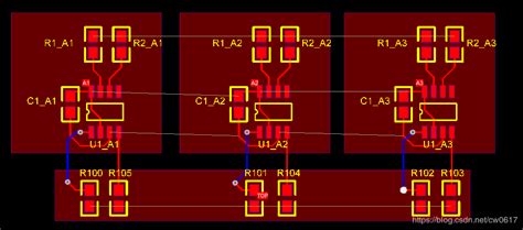
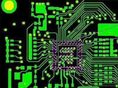
1.Follow PCB wiring rules
This is the most basic requirement for PCB designers and also the foundation. PCB wiring should generally follow the following rules:
a) The number of printed conductor wiring layers is determined according to needs. The wiring channel ratio should generally be above 50%;
b) According to the process conditions and wiring density, the wire width and wire spacing should be reasonably selected, and the wiring in the layer should be uniform and the wiring density of each layer should be similar. If necessary, auxiliary non-functional connection plates or printed wires should be added to the missing line area;
c) The wires of two adjacent layers should be arranged in a perpendicular, oblique or curved routing to reduce parasitic capacitance;
d) The printed wire wiring should be as short as possible, especially for high-frequency signals and highly sensitive signal lines; for important signal lines such as clocks, equal delay wiring should also be considered when necessary;
e) When multiple power supplies (layers) or ground (layers) are arranged on the same layer, the separation spacing should be not less than 1mm;
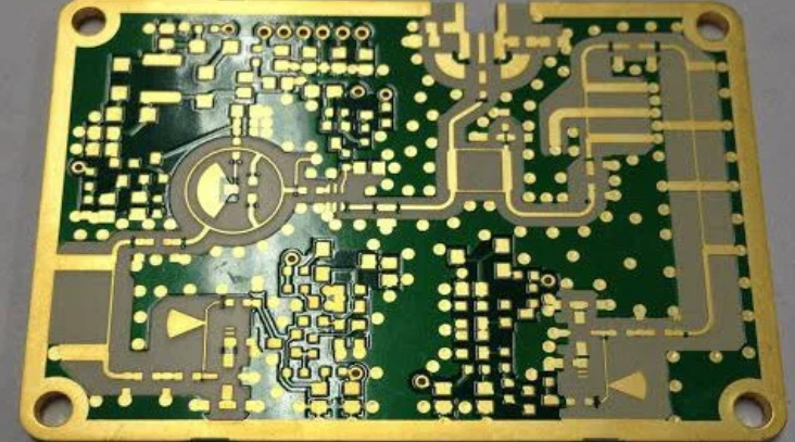
f) For large-area conductive patterns larger than 5×5mm2, windows should be opened locally;
g) Thermal isolation design should be carried out between the large-area patterns of the power layer and the ground layer and their connection plates, as shown in Figure 10, so as not to affect the welding quality;
h) Special requirements of other circuits should comply with relevant regulations.
2.Processing of power and ground wires
Even if the wiring in the entire PCB board is completed well, the interference caused by the inconsiderate consideration of the power and ground wires will reduce the performance of the product, and sometimes even affect the success rate of the product. Therefore, the wiring of the power and ground wires should be taken seriously, and the noise interference generated by the power and ground wires should be reduced to a minimum to ensure the quality of the product.
For every engineer engaged in the design of electronic products, the cause of the noise between the ground wire and the power wire is understood. Now only the reduction method of noise suppression is described: it is well known that a decoupling capacitor is added between the power and ground wires.
Try to widen the width of the power and ground wires. It is best that the ground wire is wider than the power wire. Their relationship is: ground wire>power wire>signal wire. Usually the signal wire width is: 0.2~0.3mm, the finest width can reach 0.05~0.07mm, and the power wire is 1.2~2.5mm.
For the PCB of digital circuit, a wide ground conductor can be used to form a loop, that is, to form a ground network. The ground of analog circuit cannot be used in this way. A large area of copper layer is used as the ground wire, and all unused places on the printed circuit board are connected to the ground as the ground wire. Or it can be made into a multi-layer board, with the power supply and ground wire occupying one layer each.

3.Common ground processing of digital circuits and analog circuits
Nowadays, many PCBs are no longer single-function circuits, but are composed of a mixture of digital circuits and analog circuits. Therefore, when wiring, it is necessary to consider the problem of mutual interference between them, especially the noise interference on the ground wire.
The frequency of digital circuits is high, and the sensitivity of analog circuits is strong. For signal lines, high-frequency signal lines should be as far away from sensitive analog circuit devices as possible. For ground wires, the entire PCB has only one node to the outside world, so the problem of digital and analog common ground must be processed inside the PCB. In fact, the digital ground and analog ground are separated inside the board. They are not connected to each other, but only at the interface where the PCB is connected to the outside world (such as plugs, etc.).
There is a short circuit between the digital ground and the analog ground. Please note that there is only one connection point. There are also some that do not share the same ground on the PCB, which is determined by the system design.
4.Signal lines are laid on the power layer or ground layer
When wiring a multi-layer printed circuit board, since there are not many lines left in the signal line layer, adding more layers will cause waste and increase the workload of production, and the cost will increase accordingly. To solve this contradiction, you can consider wiring on the power layer or ground layer.
First, consider using the power layer, and then the ground layer. Because it is best to preserve the integrity of the ground layer.
5.Design Rule Check (DRC)
After the wiring design is completed, it is necessary to carefully check whether the wiring design complies with the rules set by the designer, and also to confirm whether the rules set meet the requirements of the printed circuit board production process. Generally, the following aspects are checked:
a) Whether the distance between lines, lines and component pads, lines and through holes, component pads and through holes, and through holes is reasonable and meets production requirements.
b) Whether the width of the power line and the ground line is appropriate. Whether the power and ground lines are tightly coupled. Is there any place in the PCB where the ground line can be widened?
c) Have the best measures been taken for the key signal lines, such as the shortest length, adding protection lines, and clearly separating the input and output lines?
d) Do the analog circuit and digital circuit parts have their own independent ground lines? Will the graphics added to the PCB later (such as icons, annotations) cause signal short circuits?
e) Modify some undesirable line shapes.
f) Are there process lines added to the PCB? Does the solder mask meet the requirements of the production process? Is the solder mask size appropriate? Is the character mark pressed on the device pad to avoid affecting the quality of the electrical equipment?
g) Is the outer frame edge of the power ground layer in the multilayer board reduced? If the copper foil of the power ground layer is exposed outside the board, it is easy to cause a short circuit. The above is an analysis of the method to break through the bottleneck of the wiring level, and I hope it can help you.