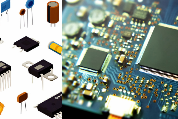
Does PCB design need 3D capabilities?
In recent years, the increase in the number of nets, tighter design constraints and routing density, and the gradual migration to high-speed, high-density projects have increased the complexity of PCBs. Fortunately, PCB design tools have been steadily evolving in recent years to meet the challenges of this increasingly complex design field. One major change – the adoption of 3D capabilities – is expected to enable designers to balance design innovation with competitiveness in the global market.
Challenges of 3D Design
Traditionally, circuit board designers have relied on design prototypes to ensure the form, fit, and functionality of the design before manufacturing. Although feasible, this approach has many disadvantages.
First, designers cannot be sure that the board will fit before the actual prototype is manufactured.
Second, this approach generally results in multiple prototypes being made during the design process.
Furthermore, multiple prototypes are very time-consuming, and the average cost of a prototype for a moderately complex design is $8,929.
It is not difficult to understand why this approach is unpopular, as any additional time or cost in the design process not only affects a company’s competitiveness, but also hinders our entry into new business.
Another drawback is that PCB design has traditionally been a 2D design. Basically, the design is created in 2D, annotated manually, and passed to the mechanical design engineer.
The mechanical engineer redraws the design in 3D using mechanical CAD software. This method is time-consuming and error-prone because it is a completely manual process.
As a result, it does not provide a competitive differentiator for designing the next generation of electronic products. It is now clear that board designers need to find better ways to view and analyze their increasingly complex designs.
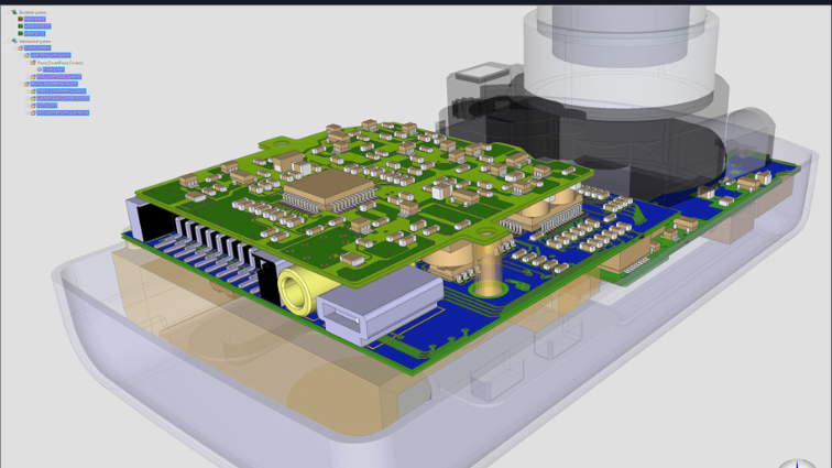
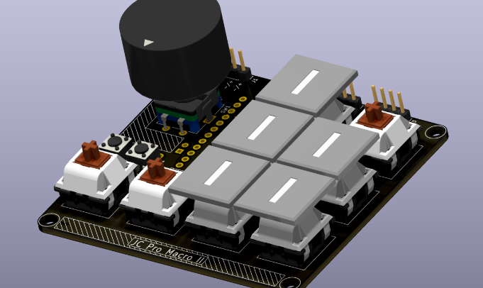
The ultimate goal of PCB designers is to create products for the real world (with 3 dimensions), so the best solution is to use a design tool with advanced 3D capabilities.
It allows designers to view the design in true 3D before production, eliminating the need to build prototypes, saving time and money. Accurate 3D models can be easily generated and then used to layout the board in true 3D.
In addition, a 3D model of the target enclosure can be imported into the PCB design to ensure that the designed board will fit perfectly into this housing. Finally, designers can submit their design files for production with confidence.
3D export capabilities provide designers with the ability to perform further analysis in other analysis tools, such as thermal analysis and electromagnetic simulation. This is critical for today’s wireless, compact, battery-powered devices, where thermal performance is completely dependent on the shape of the board.
Because of these capabilities, 3D capabilities in PCB design tools are absolutely essential for the rapid, accurate, and cost-effective design of next-generation electronic products.
Full 3D Capabilities
The value of adding 3D capabilities to PCB design is undeniable, so many companies are now promoting this capability as a selling point. However, the 3D capabilities provided by these design tools vary greatly.
To realize the full benefits of 3D, it is not enough to simply enable the viewing of true 3D images, but to expand to full 3D capabilities, including:
With this feature, designers can easily share and showcase their product designs, and even use them as marketing materials.
It can also promote better collaboration with other design teams or manufacturers. For example, with a 3D video, designers can show manufacturers what the product will look like after assembly, and the video can also be used to illustrate the order in which components are soldered to the board.
The ability to import 3D models (including components) into board designs
Note that some design tools lack this capability, allowing designers to perform only basic visualization and component clearance checks in 2D.
However, being able to import enclosures and other mechanical objects can ensure that components are placed in the right place the first time.
The ability to support 3D checking in design rules
This is a very important feature since rules are a real-time guide during the design process.
A 3D design rule checker can tell designers if there is interference in 3D space (on all axes) between two components, between a component and the enclosure, or between a component and the heat sink.
The ability to model copper layers in the PCB inner structure
Even with an ECAD package that has 3D capabilities, problems can still occur during the manufacturing process.
Finding problems at this late stage of the design can significantly increase costs. The ability to model copper layers in the PCB inner structure allows designers to easily view and verify pin connections to inner layers or thermal reliefs.
Benefits of 3D Design
Designing in 3D provides you with many benefits. It can shorten the design cycle by reducing the MCAD and ECAD iteration loop to one (or zero in some cases), and minimize design errors, greatly improving production efficiency.
And, by eliminating the uncertainty of the board layout and the housing, it allows designers to focus on the design of the product aesthetics.
Other benefits of 3D design are:
Competitive advantage
By improving communication within an organization and between suppliers and customers, 3D design can speed up product design, make the manufacturing process more reasonable and efficient, and accelerate product introduction.
Design costs are reduced, profit margins are increased, and faster time to market and improved product quality mean increased revenue.
Improve global cooperation
A true 3D design image can improve communication efficiency with suppliers, customers and manufacturers. It even allows non-CAD personnel to participate in the process (for example, for customer questionnaires, clear instructions or product configuration).
This is particularly important at a time when many companies tend to outsource production (in China or locally). Regardless of the design intent or desired end product, global design and manufacturing are extremely prone to errors and misunderstandings.
3D design images provide a common, easy-to-understand platform that all team members can operate.
More efficient design review and modification
The ability to create 3D renderings and animations simplifies the tasks of writing design plans and reviewing designs among design team members.
It also allows designers to easily implement modifications and update the latest design changes. For example, once the changes or modifications are completed, a new 3D rendering or animation can be easily generated.
More efficient manufacturing and assembly process
3D models provide a common foundation that manufacturers can work from, while also being able to more accurately and clearly communicate design intent and related design details.
Errors that were previously only discovered after production can be discovered early in the design process. As a result, the use of 3D models to manufacture and assemble products will be more accurate and efficient.
Boost Sales and Drive Marketing
A 3D model of a product can be a valuable marketing tool, allowing customers to see the full picture of the product before it is manufactured, so the sales department can quickly make market assessment reports, which can help us bring in additional revenue.
Conclusion
For many years, real-time 3D graphics technology has completely changed the way society interacts with computers. Through 3D PCB design tools, this change has now come to the PCB design field. It is changing the way electronic products are designed and manufactured.
However, as with any new technology or method, it is very important to find the best implementation and use. For PCB designers who want to benefit from 3D, this means choosing a software solution that can provide full 3D capabilities.
This solution provides the functions that circuit board designers need to help them create competitive next-generation electronic products in an increasingly complex design environment.