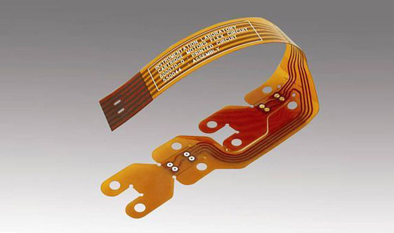
Double sided flex pcb
Advantages Of Double Sided Flex PCB In Modern Electronics
Double sided flexible printed circuit boards (PCBs) have become increasingly integral to the advancement of modern electronics, offering a multitude of advantages that cater to the evolving demands of contemporary technology. These PCBs, characterized by their ability to accommodate conductive pathways on both sides of a flexible substrate, present a unique combination of flexibility, durability, and efficiency that traditional rigid PCBs cannot match.
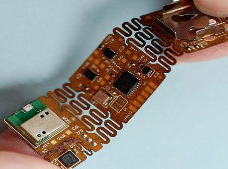
One of the primary advantages of double-sided flex PCBs is their remarkable flexibility.
This attribute allows for the design of electronic devices that can be bent, folded, or twisted without compromising their functionality. Consequently, they are ideal for applications in compact and complex devices where space constraints are a significant concern. For instance, in wearable technology, medical devices, and portable electronics, the ability to conform to various shapes and contours is invaluable. This flexibility not only enhances the ergonomic design of these devices but also contributes to their overall miniaturization, a critical factor in the competitive electronics market.
In addition to their flexibility, double-sided flex PCBs offer superior reliability and durability.
The use of flexible substrates such as polyimide or polyester provides excellent resistance to thermal and mechanical stress. This resilience ensures that the circuits can withstand repeated flexing and bending, which is essential for applications subjected to constant movement or vibration. Moreover, the materials used in these PCBs are often resistant to harsh environmental conditions, including extreme temperatures and exposure to chemicals, further extending their lifespan and reliability in demanding applications.
Another significant advantage of double-sided flex PCBs is their potential for enhanced electrical performance.
By utilizing both sides of the substrate, designers can create more complex and dense circuit layouts without increasing the overall size of the PCB. This capability is particularly beneficial in high-speed and high-frequency applications, where minimizing signal interference and maintaining signal integrity are crucial. The reduced need for interconnections and vias also contributes to lower electrical resistance and inductance, resulting in improved performance and efficiency of the electronic device.
Furthermore, double-sided flex PCBs contribute to cost savings in both manufacturing and assembly processes.
The ability to integrate multiple components and functions into a single flexible board reduces the need for additional connectors and cables, simplifying the overall design and assembly. This integration not only lowers material costs but also decreases assembly time and labor expenses. Additionally, the reduced weight and volume of these PCBs can lead to lower shipping and handling costs, further enhancing their economic viability.
The versatility of double-sided flex PCBs also extends to their application in various industries.
In the automotive sector, they are used in advanced driver-assistance systems (ADAS), infotainment systems, and lighting solutions, where their flexibility and reliability are paramount. In the aerospace industry, their lightweight and durable nature make them suitable for use in avionics and satellite systems. The medical field benefits from their application in diagnostic and monitoring devices, where precision and reliability are critical. Even in consumer electronics, double-sided flex PCBs are found in smartphones, tablets, and other portable gadgets, underscoring their widespread utility.
In conclusion, the advantages of double-sided flex PCBs in modern electronics are manifold, encompassing flexibility, durability, enhanced electrical performance, cost efficiency, and versatility. As technology continues to advance and the demand for more compact, reliable, and efficient electronic devices grows, the role of double-sided flex PCBs is poised to become even more significant. Their unique properties not only address the current challenges faced by electronic designers but also pave the way for future innovations in various industries.
Design Considerations For Double Sided Flex PCB
When designing a double-sided flexible printed circuit board (PCB), several critical considerations must be taken into account to ensure optimal performance and reliability. The unique properties of flexible PCBs, such as their ability to bend and twist, necessitate a different approach compared to traditional rigid PCBs. One of the primary factors to consider is the material selection. Flexible PCBs are typically made from polyimide or polyester substrates, which offer excellent flexibility and thermal stability. The choice of material impacts not only the mechanical properties but also the electrical performance and overall durability of the PCB.
Another crucial aspect is the layout design.
In double-sided flex PCBs, components and traces can be placed on both sides of the substrate, which allows for more complex and compact designs. However, this also introduces challenges in terms of signal integrity and electromagnetic interference (EMI). To mitigate these issues, designers must carefully plan the placement of traces and components, ensuring that high-speed signals are adequately shielded and that ground planes are strategically positioned to minimize noise.
The bending radius is another important consideration.
Flexible PCBs are designed to bend, but there are limits to how much they can flex without causing damage. The minimum bending radius is typically determined by the thickness of the PCB and the materials used. Exceeding this radius can lead to mechanical stress and potential failure of the circuit. Therefore, it is essential to design the PCB with an appropriate bending radius in mind, especially in areas where repeated flexing is expected.
Thermal management is also a key factor in the design of double-sided flex PCBs.
The flexible nature of these PCBs can make heat dissipation more challenging compared to rigid PCBs. Effective thermal management strategies, such as the use of thermal vias, heat sinks, and proper spacing of heat-generating components, are necessary to prevent overheating and ensure the longevity of the PCB.
In addition to these technical considerations, manufacturability is another critical aspect.
The fabrication process for double-sided flex PCBs is more complex than that for single-sided or rigid PCBs. It involves additional steps such as lamination, drilling, and plating, which can introduce potential defects if not carefully controlled. Therefore, it is important to work closely with the PCB manufacturer during the design phase to ensure that the design is manufacturable and that any potential issues are addressed early on.
Furthermore, the choice of adhesive materials used in the lamination process can significantly impact the performance and reliability of the double-sided flex PCB. The adhesive must provide strong bonding while maintaining flexibility and thermal stability. Poor adhesive selection can lead to delamination and failure of the PCB under mechanical stress or thermal cycling.
Finally, testing and validation are essential steps in the design process.
Double-sided flex PCBs must undergo rigorous testing to ensure that they meet the required performance specifications and can withstand the mechanical and thermal stresses they will encounter in their intended application. This includes electrical testing, thermal cycling, and mechanical bending tests.
In conclusion, designing a double-sided flexible PCB involves a comprehensive understanding of material properties, layout design, bending radius, thermal management, manufacturability, adhesive selection, and rigorous testing. By carefully considering these factors, designers can create reliable and high-performance double-sided flex PCBs that meet the demands of modern electronic applications.
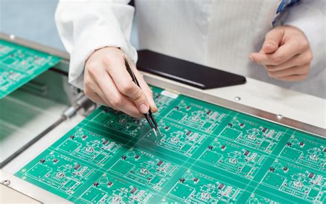
Manufacturing Process Of Double Sided Flex PCB
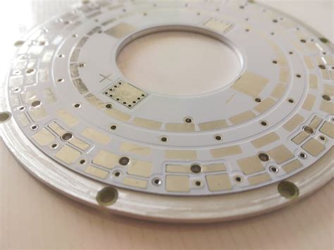
The manufacturing process of double-sided flexible printed circuit boards (PCBs) is a meticulous and intricate procedure that demands precision and expertise. This process begins with the selection of the base material, typically a polyimide film, known for its excellent thermal stability and flexibility. The polyimide film is coated with a thin layer of copper on both sides, which serves as the conductive material for the circuit.
Once the base material is prepared, the next step involves the application of a photoresist layer.
This light-sensitive material is applied to both sides of the copper-clad polyimide film. The photoresist layer is then exposed to ultraviolet (UV) light through a photomask, which contains the desired circuit pattern. The areas of the photoresist exposed to the UV light harden, while the unexposed areas remain soft and can be washed away using a developer solution. This process effectively transfers the circuit pattern onto the photoresist layer.
Following the development of the photoresist, the next stage is the etching process.
During etching, a chemical solution is used to remove the unprotected copper areas, leaving behind the desired circuit pattern. This step is crucial as it defines the electrical pathways on the double-sided flex PCB. After etching, the remaining photoresist is stripped away, revealing the copper circuit pattern on both sides of the polyimide film.
To ensure electrical connectivity between the two sides of the PCB, through-holes or vias are created.
This is achieved by drilling tiny holes at specific locations on the board. These holes are then plated with copper to establish a conductive path between the top and bottom layers. The plating process involves immersing the board in a series of chemical baths that deposit a thin layer of copper inside the drilled holes.
Subsequently, the double-sided flex PCB undergoes a series of cleaning and inspection processes to remove any residual chemicals and ensure the integrity of the circuit pattern. The board is then laminated with a protective coverlay or solder mask, which serves to insulate and protect the copper traces from environmental factors and mechanical damage. The coverlay is typically made of a flexible polyimide film that is bonded to the board using heat and pressure.
Once the coverlay is applied, the board is subjected to a final inspection to verify its electrical and mechanical properties.
This includes testing for continuity, insulation resistance, and overall dimensional accuracy. Any defects or inconsistencies are identified and rectified at this stage to ensure the final product meets the required specifications.
The final step in the manufacturing process is the cutting or routing of the double-sided flex PCB into its desired shape and size. This is done using precision cutting tools or laser cutting technology to achieve clean and accurate edges. The finished boards are then packaged and prepared for shipment to the customer.
In conclusion, the manufacturing process of double-sided flex PCBs involves a series of carefully controlled steps, each critical to achieving a high-quality and reliable product. From the selection of materials to the final inspection, every stage requires attention to detail and adherence to stringent quality standards. This ensures that the double-sided flex PCBs can meet the demanding requirements of various applications, ranging from consumer electronics to aerospace and medical devices.
Applications Of Double Sided Flex PCB In Various Industries
Double-sided flexible printed circuit boards (PCBs) have become increasingly integral to a variety of industries due to their unique combination of flexibility, durability, and compact design. These PCBs, which feature conductive layers on both sides of a flexible substrate, offer numerous advantages over traditional rigid PCBs, making them suitable for a wide range of applications. As technology continues to advance, the demand for double-sided flex PCBs is expected to grow, driven by their ability to meet the evolving needs of various sectors.
In the consumer electronics industry, double-sided flex PCBs are widely used in devices such as smartphones, tablets, and wearable technology.
The compact and lightweight nature of these PCBs allows for the design of smaller, more efficient devices without compromising on performance. For instance, in smartphones, double-sided flex PCBs enable the integration of multiple functions within a limited space, contributing to the sleek and slim designs that consumers prefer. Additionally, the flexibility of these PCBs allows for better shock absorption, enhancing the durability of electronic devices.
The automotive industry also benefits significantly from the use of double-sided flex PCBs.
Modern vehicles are equipped with a multitude of electronic systems, including advanced driver-assistance systems (ADAS), infotainment systems, and various sensors. Double-sided flex PCBs are ideal for these applications due to their ability to withstand harsh environmental conditions, such as extreme temperatures and vibrations. Moreover, their flexibility allows for easier installation in the confined spaces of a vehicle, improving overall design efficiency and reliability.
In the medical field, double-sided flex PCBs play a crucial role in the development of advanced medical devices.
These PCBs are used in diagnostic equipment, such as MRI machines and ultrasound devices, as well as in wearable health monitors and implantable devices. The flexibility and reliability of double-sided flex PCBs ensure that medical devices can be designed to be both compact and highly functional. For example, in wearable health monitors, these PCBs enable continuous monitoring of vital signs without causing discomfort to the patient, thereby improving patient compliance and health outcomes.
The aerospace and defense industries also leverage the advantages of double-sided flex PCBs.
In aerospace applications, these PCBs are used in avionics systems, satellite communications, and other critical electronic components. The ability to withstand extreme conditions, such as high altitudes and intense vibrations, makes double-sided flex PCBs an ideal choice for aerospace applications. Similarly, in the defense sector, these PCBs are used in various military equipment, including communication devices, radar systems, and unmanned aerial vehicles (UAVs). The reliability and durability of double-sided flex PCBs ensure that military equipment can perform optimally in demanding environments.
Furthermore, the industrial sector utilizes double-sided flex PCBs in automation and control systems.
These PCBs are found in robotic arms, sensors, and other machinery that require precise and reliable electronic control. The flexibility of double-sided flex PCBs allows for more efficient routing of electrical connections, reducing the overall size and weight of industrial equipment. This, in turn, enhances the performance and efficiency of automated systems, contributing to increased productivity and reduced operational costs.
In conclusion, double-sided flex PCBs have become indispensable across various industries due to their unique properties and advantages. From consumer electronics and automotive applications to medical devices, aerospace, defense, and industrial automation, these PCBs offer unparalleled flexibility, durability, and design efficiency. As technology continues to evolve, the applications of double-sided flex PCBs are expected to expand further, driving innovation and improving performance across multiple sectors.