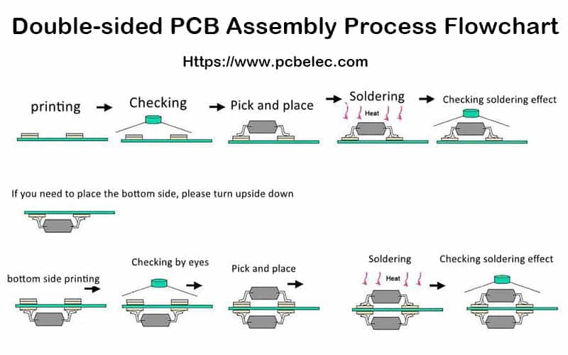
Double sided pcb assembly process
Benefits Of Double Sided PCB Assembly In Modern Electronics
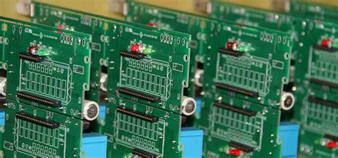
Double-sided printed circuit board (PCB) assembly has become a cornerstone in the advancement of modern electronics, offering a multitude of benefits that enhance both the functionality and efficiency of electronic devices.
One of the primary advantages of double-sided PCB assembly is the increased circuit density it provides.
By utilizing both sides of the PCB, designers can place more components in a given area, which is particularly beneficial in the development of compact and complex electronic devices. This increased density not only allows for more sophisticated circuitry but also contributes to the miniaturization of electronic products, a trend that is highly valued in today’s market.
Moreover, double-sided PCB assembly facilitates improved electrical performance.
The ability to place components on both sides of the board enables more efficient routing of electrical pathways, reducing the length of connections and thereby minimizing signal loss and interference. This is especially critical in high-frequency applications where signal integrity is paramount. Additionally, the use of vias, which are small holes that allow electrical connections between the two sides of the PCB, further enhances the performance by providing multiple pathways for current flow, thereby reducing resistance and improving overall circuit reliability.
Another significant benefit of double-sided PCB assembly is its cost-effectiveness.
While the initial design and manufacturing process may be more complex compared to single-sided PCBs, the long-term cost savings are substantial. The ability to fit more components on a smaller board reduces the need for additional PCBs, which in turn lowers material costs. Furthermore, the compact design can lead to savings in packaging and shipping, as smaller and lighter products are less expensive to transport. This cost efficiency is particularly advantageous for large-scale production runs, where even small savings per unit can accumulate to significant amounts.
In addition to cost savings, double-sided PCB assembly also offers greater design flexibility.
Engineers and designers have more options when it comes to component placement and circuit layout, allowing for more innovative and efficient designs. This flexibility is crucial in the development of cutting-edge technologies, where space constraints and performance requirements are continually pushing the boundaries of what is possible. The ability to optimize the layout on both sides of the PCB can lead to more robust and reliable products, which is a key consideration in industries such as aerospace, automotive, and medical devices.
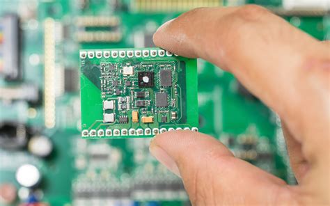
Furthermore, double-sided PCB assembly supports the integration of advanced technologies such as surface mount technology (SMT) and through-hole technology (THT).
SMT allows for the placement of smaller and more complex components, which can be mounted directly onto the surface of the PCB, while THT provides strong mechanical bonds for components that require more robust connections. The combination of these technologies on a double-sided PCB enables the creation of highly sophisticated and durable electronic devices.
In conclusion, the benefits of double-sided PCB assembly in modern electronics are manifold, ranging from increased circuit density and improved electrical performance to cost-effectiveness and greater design flexibility. These advantages make double-sided PCBs an indispensable component in the development of advanced electronic devices, driving innovation and efficiency in various industries. As technology continues to evolve, the role of double-sided PCB assembly will undoubtedly remain pivotal in meeting the ever-growing demands for smaller, faster, and more reliable electronic products.
Key Steps In The Double Sided PCB Assembly Process
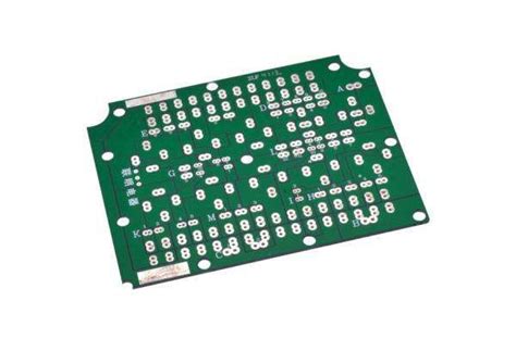
The double-sided PCB assembly process is a sophisticated procedure that involves several critical steps to ensure the functionality and reliability of the final product. This process begins with the design phase, where engineers create a detailed layout of the circuit, specifying the placement of components on both sides of the PCB. Once the design is finalized, the next step is to fabricate the bare PCB, which involves etching the copper layers to form the circuit patterns on both sides of the board.
Following the fabrication of the bare PCB, the assembly process commences with the application of solder paste.
Solder paste is a mixture of tiny solder balls and flux, which is applied to the pads where components will be mounted. This is typically done using a stencil that ensures precise application. The board is then placed in a pick-and-place machine, which accurately positions surface-mount components onto the solder paste-covered pads. This step is repeated for both sides of the PCB, requiring careful handling to avoid disturbing the components already placed on the opposite side.
Once all surface-mount components are in place, the board undergoes a reflow soldering process.
During reflow soldering, the board is passed through an oven where it is gradually heated to melt the solder paste, creating strong electrical and mechanical connections between the components and the PCB. This process must be carefully controlled to prevent overheating, which could damage sensitive components. After reflow soldering, the board is inspected to ensure that all connections are properly formed and that there are no defects such as solder bridges or cold joints.
In addition to surface-mount components, double-sided PCBs often include through-hole components, which require a different assembly technique.
Through-hole components have leads that pass through holes in the PCB and are soldered on the opposite side. This is typically done using a wave soldering process, where the board is passed over a wave of molten solder that simultaneously solders all the through-hole connections. Alternatively, selective soldering may be used for boards with a mix of surface-mount and through-hole components, allowing for precise soldering of specific areas.
After all components are soldered, the assembled PCB undergoes a series of inspections and tests to verify its functionality and quality.
Automated optical inspection (AOI) systems are commonly used to check for soldering defects, component misalignment, and other issues. Additionally, X-ray inspection may be employed to examine hidden solder joints, particularly for components with leads underneath, such as ball grid arrays (BGAs). Functional testing is also performed to ensure that the PCB operates as intended, often involving the application of power and signals to simulate real-world operating conditions.
The final steps in the double-sided PCB assembly process include cleaning and conformal coating.
Cleaning removes any residual flux and contaminants that could affect the board’s performance or reliability. Conformal coating involves applying a protective layer to the PCB to shield it from environmental factors such as moisture, dust, and chemicals. This step is particularly important for PCBs used in harsh environments.
In conclusion, the double-sided PCB assembly process is a complex and meticulous procedure that requires careful planning, precise execution, and thorough testing to ensure the production of high-quality, reliable circuit boards. Each step, from design and fabrication to assembly and inspection, plays a crucial role in achieving the desired outcome, making it essential for manufacturers to adhere to stringent standards and best practices throughout the process
Common Challenges And Solutions In Double Sided PCB Assembly
Double-sided PCB assembly is a critical process in modern electronics manufacturing, offering increased circuit density and functionality within a compact footprint. However, this complexity introduces several challenges that must be addressed to ensure reliable and efficient production.
One common challenge is the alignment of components on both sides of the PCB.
Misalignment can lead to poor solder joints, which may cause intermittent connections or complete circuit failure. To mitigate this issue, manufacturers employ precise pick-and-place machines equipped with advanced vision systems. These systems ensure accurate component placement by continuously monitoring and adjusting the position of each component during assembly.
Another significant challenge is managing thermal profiles during the reflow soldering process.
Double-sided PCBs require careful control of temperature to prevent damage to components and ensure proper solder joint formation. The reflow process must be meticulously calibrated to accommodate the thermal mass of components on both sides of the board. One effective solution is to use a two-pass reflow process, where each side of the PCB is soldered separately. This approach allows for better thermal management and reduces the risk of overheating sensitive components.
Solder paste application is also a critical aspect of double-sided PCB assembly.
Inconsistent or insufficient solder paste can lead to weak solder joints, while excessive paste can cause bridging and short circuits. To address this, manufacturers utilize high-precision stencil printing techniques and automated inspection systems. These systems ensure uniform solder paste deposition and identify any defects early in the process, allowing for immediate corrective action.
Component warpage is another challenge that can affect the quality of double-sided PCB assemblies.
Warped components may not sit flush against the PCB, leading to poor solder joints and potential reliability issues. To combat this, manufacturers often use specialized fixtures and supports during the assembly process to maintain component flatness. Additionally, selecting components with lower susceptibility to warpage and optimizing the reflow profile can further minimize this issue.
The presence of through-hole components on double-sided PCBs adds another layer of complexity.
These components require additional soldering processes, such as wave soldering or selective soldering, which must be carefully integrated into the overall assembly workflow. Ensuring proper soldering of through-hole components without disturbing surface-mounted components on the opposite side of the PCB is a delicate balancing act. One solution is to use selective soldering techniques, which precisely target through-hole leads while avoiding nearby surface-mounted components.
Inspection and testing of double-sided PCBs present unique challenges as well.
Traditional inspection methods, such as visual inspection and automated optical inspection (AOI), may not be sufficient to detect all potential defects on both sides of the board. To enhance inspection accuracy, manufacturers often employ X-ray inspection systems, which can reveal hidden defects such as voids, solder bridges, and misaligned components. Additionally, implementing in-circuit testing (ICT) and functional testing ensures that the assembled PCB meets all performance and reliability requirements.
In conclusion, while double-sided PCB assembly offers significant advantages in terms of circuit density and functionality, it also presents a range of challenges that must be carefully managed. Through the use of advanced technologies and meticulous process control, manufacturers can overcome these challenges and produce high-quality, reliable double-sided PCBs. By continuously refining assembly techniques and leveraging innovative solutions, the industry can meet the growing demands of modern electronic devices.
Innovations In Double Sided PCB Assembly Technology
The double-sided PCB assembly process has undergone significant innovations in recent years, driven by the increasing demand for more compact, efficient, and reliable electronic devices. As technology continues to evolve, manufacturers are constantly seeking ways to enhance the performance and functionality of printed circuit boards (PCBs).
One of the most notable advancements in this field is the development of double-sided PCB assembly technology, which allows for the placement of electronic components on both sides of the board. This innovation has revolutionized the electronics industry, enabling the creation of more complex and powerful devices.
To begin with, the double-sided PCB assembly process involves several critical steps, each of which has been refined through technological advancements. Initially, the PCB is designed using sophisticated computer-aided design (CAD) software, which allows engineers to create intricate layouts with high precision. This design phase is crucial, as it ensures that the final product will meet the desired specifications and performance requirements. Once the design is complete, the PCB is fabricated using advanced manufacturing techniques, such as photolithography and etching, to create the necessary conductive pathways on both sides of the board.
Following the fabrication of the PCB, the next step in the assembly process is the application of solder paste. This is typically done using a stencil and a squeegee to ensure that the solder paste is applied evenly and accurately to the designated areas. The solder paste serves as an adhesive that will hold the electronic components in place during the subsequent reflow soldering process. With the solder paste applied, the components are then placed onto the PCB using automated pick-and-place machines, which are capable of positioning components with remarkable speed and precision.
One of the key innovations in double-sided PCB assembly technology is the development of advanced reflow soldering techniques. Traditionally, reflow soldering was performed in a single pass, which limited the ability to place components on both sides of the PCB. However, modern reflow soldering ovens are now equipped with multiple heating zones and advanced temperature control systems, allowing for the sequential soldering of components on both sides of the board. This has significantly improved the efficiency and reliability of the assembly process, as it reduces the risk of component displacement and solder joint defects.
In addition to reflow soldering, another important advancement in double-sided PCB assembly technology is the use of through-hole and surface-mount technology (SMT) components. Through-hole components, which have leads that pass through the PCB and are soldered on the opposite side, provide robust mechanical connections and are ideal for high-stress applications. On the other hand, SMT components are mounted directly onto the surface of the PCB, allowing for greater component density and more compact designs. The integration of both through-hole and SMT components in double-sided PCB assembly has enabled manufacturers to create highly sophisticated and reliable electronic devices.
Furthermore, the inspection and testing of double-sided PCBs have also seen significant improvements. Automated optical inspection (AOI) systems and X-ray inspection machines are now commonly used to detect defects and ensure the quality of the assembled PCBs. These advanced inspection techniques provide a high level of accuracy and reliability, helping to identify issues that may not be visible to the naked eye.
In conclusion, the innovations in double-sided PCB assembly technology have greatly enhanced the capabilities of electronic devices, allowing for more complex and efficient designs. From advanced reflow soldering techniques to the integration of through-hole and SMT components, these advancements have streamlined the assembly process and improved the overall quality and reliability of PCBs. As technology continues to advance, it is likely that we will see even more groundbreaking developments in the field of double-sided PCB assembly, further pushing the boundaries of what is possible in the world of electronics.