Double-Sided SMT Assembly: A Comprehensive Guide
Introduction
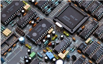
Surface Mount Technology (SMT) has revolutionized the electronics manufacturing industry by enabling the production of smaller, faster, and more reliable electronic devices. One of the key advancements in SMT is double-sided assembly, which allows components to be mounted on both sides of a Printed Circuit Board (PCB). This technique maximizes the use of available board space, enabling higher component density and more complex circuit designs. Double-sided SMT assembly is widely used in applications ranging from consumer electronics to automotive systems and medical devices. This article provides an in-depth exploration of double-sided SMT assembly, covering its benefits, challenges, processes, and best practices.
1. What is Double-Sided SMT Assembly?
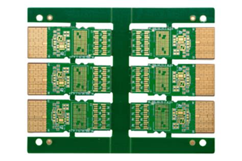
Double-sided SMT assembly refers to the process of mounting surface-mount components on both the top and bottom sides of a PCB. This technique is particularly useful for complex designs where space is limited, and a high density of components is required. By utilizing both sides of the board, designers can create more compact and efficient electronic devices without compromising functionality.
Double-sided SMT assembly is commonly used in applications such as:
- Smartphones and tablets
- Laptops and computers
- Automotive control systems
- Medical devices
- IoT (Internet of Things) devices
2. Benefits of Double-Sided SMT Assembly
Double-sided SMT assembly offers several advantages over single-sided assembly, making it a preferred choice for many modern electronic designs.
2.1 Increased Component Density
By utilizing both sides of the PCB, double-sided assembly allows for a higher density of components. This is particularly important for compact devices such as smartphones and wearables, where space is at a premium.
2.2 Improved Design Flexibility
Double-sided assembly provides greater flexibility in circuit design, enabling engineers to create more complex and sophisticated layouts. This is especially beneficial for high-performance applications that require advanced functionality.
2.3 Reduced PCB Size
With components mounted on both sides, the overall size of the PCB can be reduced. This not only saves space but also reduces material costs and makes the final product more portable.
2.4 Enhanced Performance
Double-sided assembly can improve the electrical performance of a PCB by reducing the length of signal traces and minimizing parasitic inductance and capacitance. This is critical for high-speed and high-frequency applications.
3. Challenges of Double-Sided SMT Assembly
While double-sided SMT assembly offers numerous benefits, it also presents several challenges that must be addressed to ensure successful production.
3.1 Component Placement and Orientation
Mounting components on both sides of the PCB requires careful planning to avoid interference between components on the top and bottom layers. Components must be oriented and placed in a way that minimizes the risk of mechanical or electrical conflicts.
3.2 Soldering Process
The soldering process for double-sided assembly is more complex than for single-sided assembly. Components on the bottom side of the board must be securely soldered without disturbing the components on the top side. This often requires multiple reflow soldering cycles, which can increase the risk of defects such as tombstoning or solder bridging.
3.3 Thermal Management
Double-sided assembly can lead to increased heat generation, especially in high-density designs. Proper thermal management is essential to prevent overheating and ensure the reliability of the final product.
3.4 Inspection and Testing
Inspecting and testing double-sided PCBs is more challenging due to the increased complexity of the design. Automated Optical Inspection (AOI) and X-ray inspection are often required to detect defects such as insufficient solder joints or misaligned components.
4. Double-Sided SMT Assembly Process
The double-sided SMT assembly process involves several key steps, each of which must be carefully executed to ensure high-quality results.
4.1 Solder Paste Application
The first step in the assembly process is the application of solder paste to the PCB. This is typically done using a stencil that ensures the solder paste is applied only to the designated pads. For double-sided assembly, solder paste is applied to one side of the board at a time.
4.2 Component Placement
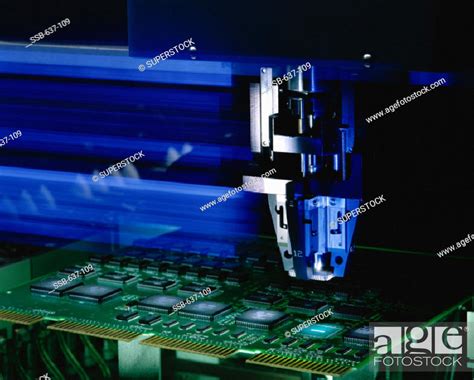
Once the solder paste has been applied, the components are placed onto the PCB using automated pick-and-place machines. For double-sided assembly, the components on the first side (usually the bottom side) are placed and soldered before the process is repeated for the second side.
4.3 Reflow Soldering
After the components have been placed, the PCB is passed through a reflow oven. The reflow oven heats the board to a temperature that melts the solder paste, creating a strong electrical and mechanical connection between the components and the PCB. For double-sided assembly, the reflow process is performed twice—once for each side of the board.
4.4 Inspection and Testing
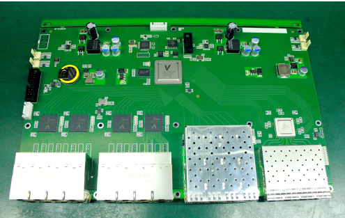
After the soldering process is complete, the assembled PCB undergoes inspection and testing to ensure that all components are correctly placed and soldered, and that the circuit functions as intended. Inspection methods include visual inspection, AOI, and X-ray inspection, while functional testing ensures that the PCB performs its intended function.
5. Best Practices for Double-Sided SMT Assembly
To achieve high-quality results in double-sided SMT assembly, it is important to follow best practices throughout the design and manufacturing process.
5.1 Design Considerations
- Component Placement: Carefully plan the placement of components on both sides of the PCB to avoid interference and ensure proper soldering.
- Thermal Management: Incorporate thermal vias, heat sinks, and other cooling solutions to manage heat dissipation in high-density designs.
- Signal Integrity: Minimize the length of signal traces and use proper grounding techniques to reduce noise and improve performance.
5.2 Process Optimization
- Reflow Profile: Optimize the reflow soldering profile to ensure proper melting of the solder paste without damaging the components.
- Stencil Design: Use high-quality stencils with precise apertures to ensure accurate solder paste application.
- Inspection and Testing: Implement robust inspection and testing procedures to detect and address defects early in the production process.
5.3 Material Selection
- PCB Material: Choose high-quality PCB materials that can withstand the thermal and mechanical stresses of double-sided assembly.
- Solder Paste: Use solder paste with the appropriate composition and particle size for the specific application.
6. Applications of Double-Sided SMT Assembly
Double-sided SMT assembly is used in a wide range of applications across various industries. Some of the most common applications include:
6.1 Consumer Electronics
Smartphones, tablets, laptops, and other consumer electronics often use double-sided SMT assembly to achieve high component density and compact designs.
6.2 Automotive Systems
Modern vehicles rely on double-sided SMT assembly for advanced control systems, infotainment systems, and sensors.
6.3 Medical Devices
Medical devices such as imaging equipment, diagnostic tools, and wearable monitors benefit from the compact and reliable designs enabled by double-sided SMT assembly.
6.4 Industrial Equipment
Industrial automation systems, robotics, and control systems often use double-sided SMT assembly to achieve high performance and reliability.
6.5 IoT Devices
The growing Internet of Things (IoT) industry relies on double-sided SMT assembly to produce compact and energy-efficient devices for smart homes, wearables, and industrial applications.
7. Future Trends in Double-Sided SMT Assembly
As technology continues to evolve, double-sided SMT assembly is expected to play an increasingly important role in electronics manufacturing. Some of the key trends shaping the future of double-sided SMT assembly include:
7.1 Miniaturization
The demand for smaller and more compact devices is driving the development of advanced SMT techniques, including double-sided assembly. As components continue to shrink, double-sided assembly will become even more critical for achieving high component density.
7.2 Advanced Materials
The use of advanced materials, such as high-performance PCB substrates and lead-free solder, is expected to increase in double-sided SMT assembly. These materials offer improved thermal and electrical properties, enabling higher performance and reliability.
7.3 Automation and AI
Automation and artificial intelligence (AI) are being integrated into the SMT assembly process to improve efficiency, accuracy, and quality. Automated inspection systems, AI-driven process optimization, and robotic assembly are expected to become more widespread in double-sided SMT assembly.
7.4 Sustainability
The electronics industry is increasingly focused on sustainability, and double-sided SMT assembly is no exception. Manufacturers are adopting green practices, such as recycling materials, reducing energy consumption, and using environmentally friendly solder, to minimize the environmental impact of their operations.
Conclusion
Double-sided SMT assembly is a critical technology in modern electronics manufacturing, enabling the production of compact, high-performance, and reliable devices. By mounting components on both sides of the PCB, designers can achieve higher component density, improved design flexibility, and enhanced performance. While double-sided assembly presents certain challenges, such as component placement, soldering, and inspection, these can be addressed through careful planning, process optimization, and the use of advanced technologies. As the electronics industry continues to evolve, double-sided SMT assembly will remain at the forefront of innovation, driving the development of next-generation devices across a wide range of applications.

