EDA technology and FPGA design application
Introduction
The 21st century is a knowledge economy era dominated by the electronic information industry. A great change is taking place in the information field, and its leading force and decisive factor are microelectronic integrated circuits. The increasing maturity of silicon chip technology, especially deep submicron (DSM) and very deep submicron (VDSM) technology, has greatly promoted the rapid development of the integrated circuit industry.
The development of integrated circuits has gone through circuit integration, function integration, and technology integration, and today is based on computer software and hardware knowledge integration, which marks that traditional electronic systems have fully entered the modern electronic system stage, which is also known as entering the 3G era, that is, the single-chip integration reaches 1G transistors, the device operating speed reaches 1GHz, and the data transmission rate reaches 1Gbps.
EDA (Electronic Design Automation) technology is based on computer-aided design. It integrates the latest achievements of applied electronic technology, computer technology, information processing technology, and intelligent technology to realize the automatic design of electronic products. EDA is the core of modern electronic design technology and occupies an important position in modern integrated circuit design. FPGA (Field Programmable Gate Array) is a typical representative of programmable logic devices. Its emergence and increasing perfection have adapted to the wave of digital development in today’s era. It is widely used in modern digital system design.
EDA technology and FPGA principles
1.EDA technology features
EDA is a revolution in the field of electronic design. It originated from computer-aided design (CAD, Computer Aided Design), computer-aided manufacturing (CAM, Computer Aided Made), computer-aided testing (CAT, Computer Aided Test) and computer-aided engineering (CAE, Computer Aided Engineering). Using EDA tools, electronic designers design electronic systems from concepts, algorithms, and protocols. The entire process from circuit design, performance analysis to IC layout or PCB layout generation can be automatically completed on the computer.
EDA represents the latest development direction of electronic design technology today.
Its basic feature is that designers use computers as tools to design and divide the entire system according to the top-down design method, complete the system behavior level design by hardware description language, and use advanced development tools to automatically complete logic compilation, simplification, segmentation, synthesis, optimization, layout and routing (PAR, Place And Route), simulation and adaptation compilation and programming download of specific target chips. This is called a high-level design method for digital logic circuits.
As the leading technology for modern electronic system design, EDA has two obvious characteristics: concurrent engineering design and top-down design. Its basic idea is to start from the overall requirements of the system, divided into three levels: behavior description (Behaviour Description), register transfer level (RTL, Register Transfer Level) description, and logic synthesis (Logic Synthesis), gradually refine the design content, and finally complete the overall design. This is a new design idea and design concept.
2.FPGA Principle
Today, the design methods and means of digital electronic systems have undergone fundamental changes, and are shifting from discrete digital circuits to programmable logic devices (PLD) and application-specific integrated circuits (ASIC). Both FPGA and CPLD (Programmable Logic Device) belong to the category of PLD, and they are playing an increasingly important role in modern digital system design.
FPGA is a digital integrated circuit that is programmed by the user to implement the required logic functions. It not only has the advantages of flexible design, high performance, and fast speed, but also has a short time to market and low cost. FPGA design is very similar to ASIC front-end design. FPGA applications are becoming increasingly popular in the semiconductor field and have become the most dynamic and promising industry in integrated circuits. At the same time, with the improvement of design technology and manufacturing processes, device performance, integration, operating frequency and other indicators are constantly improving, and FPGA has increasingly become the first choice for system-level chip design.
FPGA is developed from PAL (Programmable Array Logic) and GAL (General Array Logic). Its basic design concept is to use EDA development tools to describe system functions and algorithms using schematics, state machines, Boolean expressions, hardware description languages, etc., to design and implement and generate programming files, and finally implement them with target devices through programmers or download cables.
FPGA devices use logic cell array (LCA) structure and SDRAM process, where LCA consists of three types of programmable units.
(1) Configurable logic block (CLB): called the core array, it is the basic unit for implementing custom logic functions and is scattered throughout the chip;
(2) Input/output block (IOB): arranged around the chip, providing a programmable interface between the internal logic and the device package pins;
(3) Programmable interconnect resources (PI): including wire segments of different lengths and connection switches, whose function is to connect various programmable logic blocks or I/O blocks to form a specific circuit.
There are many manufacturers of FPGAs in the world, but the most influential ones are Xilinx and Altera. The world’s first FPGA was first launched by Xilinx in the mid-1980s. FPGAs produced by different manufacturers have large differences in the scale of programmable logic blocks, internal interconnection structure and programmable components used. They should be distinguished in actual use.
FPGA design application and optimization strategy
1.FPGA design level analysis
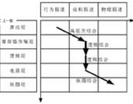
FPGA design includes two aspects: description level and description field. Usually, the design description is divided into 6 abstract levels, from high to low: system level, algorithm level, register transfer level, logic level, circuit level and layout level. There are three different fields of description for each layer: behavior domain description, structure domain description and physical domain description.
The system level is the highest level of abstract description of the system, targeting the overall performance of the electronic system. The algorithm level is also called the behavior level, which is a functional description of each module after system-level performance analysis and structural division. The functions and behaviors described in the algorithm level are ultimately implemented by digital circuits. Digital circuits can essentially be considered to be composed of registers and combinational logic circuits, where registers are responsible for signal storage and combinational logic circuits are responsible for signal transmission. The register transfer layer description describes the entire system from the perspective of signal storage and transmission. Registers and combinational logic are essentially composed of logic gates, and the logic layer describes the entire system from the perspective of logic gate combination and connection.
The relationship between the various description levels and synthesis technologies of FPGA is shown in Figure 1. Traditional synthesis tools convert the description of the register transfer level (RTL) into a gate-level description. With the continuous maturity of the new generation of system design theory with behavioral design as the main feature, high-level synthesis technologies that can convert system behavioral level descriptions into RTL descriptions continue to emerge.
As the focus and hot spot of modern integrated circuit design, FPGA design generally adopts a top-down, coarse-to-fine, and step-by-step refinement approach. The top level of design refers to the overall requirements of the system, and the bottom level refers to the specific logic circuit implementation. Top-down is to gradually decompose the entire digital system into various subsystems and modules. If the subsystem is large in scale, it is further decomposed into smaller subsystems and modules, layer by layer, until the relationship between the submodules in the entire system is reasonable and easy to design and implement.
2.Application of VHDL in FPGA Design
The scale and complexity of integrated circuit design are increasing. The traditional schematic diagram method for system-level chip design can no longer meet the design requirements. Hardware Description Language (HDL) has many advantages in large-scale digital system design. Therefore, the use of hardware description language for system behavior level design has become the mainstream of FPGA and ASIC design. Currently, the most popular and representative hardware description languages are VHDL (VHSIC Hardware Description Language) developed by the US Department of Defense (DOD) and Verilog HDL developed by GDA (Gateway Design Automation).
VHSIC stands for Very High Speed Integrated Circuit, so VHDL is the hardware description language for very high speed integrated circuits. VHDL has strict syntax and became an IEEE standard in 1987, namely IEEE STD 1076-1987, and was further revised to IEEE STD 1076-1993 in 1993.
As an IEEE standard, VHDL has been supported by many EDA companies. Its main advantages are:
● Strong description ability, supporting three levels of design: system behavior level, register transfer level and gate level;
● Good readability and strong portability. Its source file is both a program and a document, which is easy to reuse and communicate;
● Supports top-down design and library-based design;
● Supports the design of synchronous, asynchronous and random circuits;
● It is independent of the process and has a long life cycle.
VHDL language is mainly used in the behavior layer and register transfer layer. These two layers can give full play to the advantages of VHDL facing the high level. The essence of using VHDL to realize digital circuits is to use synthesis tools to convert high-level descriptions into low-level gate-level descriptions. The synthesis can be divided into three levels: high-level synthesis, logic synthesis and layout synthesis.
3.FPGA system behavior level design based on VHDL
The basic process and detailed process of FPGA design based on VHDL are shown in Figure 2 and Figure 3 respectively, which specifically include the following important links: design entry, design synthesis, design constraints, design implementation, design simulation and device programming.
Design entry mainly uses HDL (hardware description language), ECS (Engineering Schematic Capture, schematic editor) and FSM (Finite State Machine);
Design synthesis is to optimize the HDL file into a hardware circuit implementation scheme based on the logic design description and constraints using development tools. Its essence is the process of optimizing the design goal;
Design constraints mainly include design rule constraints, time constraints and area constraints. Usually, time constraints have a higher priority than area constraints;
Design implementation for FPGA is divided into compilation planning, layout and routing (PAR, Place And Route), and program bitstream file generation; for CPLD, it is compilation, configuration, and bitstream file generation;
Design simulation is divided into functional simulation and timing delay simulation. Functional simulation is performed after design input and before synthesis, and only functional verification is performed, also known as pre-simulation. Timing delay simulation is performed after synthesis and layout and routing, and can obtain detailed timing delay information of the target device, also known as post-simulation;
Device programming refers to downloading the bit stream formed after synthesis to a specific FPGA/CPLD chip under the premise that functional simulation and timing delay simulation are correct, also known as chip configuration. FPGA/CPLD programming downloads can usually use three methods: JTAG programmer, PROM file formatter and hardware debugger. Among them, JTAG (Joint Test Action Group) is the access interface of the industrial standard IEEE 1149.1 boundary scan test. When used as a programming function, it can save dedicated programming interfaces and reduce system pinouts, which is conducive to the unification of programming interfaces of various programmable logic devices, so it is widely used.
4.FPGA design optimization and solution improvement
In FPGA design, it must be made clear that HDL source code writing is very important; different synthesis tools contain different synthesis subsets, which makes some HDL statements unable to be synthesized in some synthesis tools; the same logic function can be described by different HDL statements, but the occupied resources may be very different. At the same time, we should deeply understand that concurrency is the fundamental difference between hardware description language and ordinary high-level language, so the design of hardware circuits cannot be bound by traditional sequential execution thinking.
In addition, we should be clear that speed optimization and area optimization play an important role in FPGA design. For most digital system designs, speed is often the first requirement, but FPGA structural characteristics, synthesis tool performance, system circuit composition, PCB plate making and HDL code expression will have an important impact on the working speed. We can optimize speed by using pipeline design, register balancing and critical path method in circuit structure design.
(1) Pipeline design
Pipelining technology is quite popular in speed optimization. It can significantly improve the upper limit of the operating speed of the system design. Pipelining technology is indispensable in the design of modern microprocessors, digital signal processors, MCU single-chip computers, and high-speed digital systems. Figures 4 and 5 are typical diagrams of pipeline design. Figure 4 does not use pipeline design, while Figure 5 uses a two-stage pipeline design. In the design, the combinational logic block with a larger delay is cut into two combinational logic blocks with roughly equal delays, and triggers are inserted into these two logic blocks, that is, the following relationship is satisfied: Ta=T1+T2, T1≈T2. Through analysis, it can be seen that Fmax≈1/Ta in Figure 4; the maximum operating frequency of the first stage of the pipeline in Figure 5 is Fmax1≈1/T1, and the maximum operating frequency of the second stage of the pipeline is Fmax2≈1/T2≈1/T1. The total design maximum frequency isFmax≈Fmax1≈Fmax2≈1/T1, so the design speed of Figure 5 is nearly doubled compared to Figure 4. The working principle of the pipeline can be shown in Figure 6.
(2) Register Balancing
Register balancing is to achieve speed optimization by balancing the combinational delay logic blocks between registers, as shown in Figures 7 and 8. The delay difference between the two combinational logic blocks in Figure 7 is too large, resulting in the overall operating frequency Fmax of the design depending on T1, that is, the largest delay module, which limits the overall performance of the design. By improving the design of Figure 7, part of the logic of combinational logic 1 with a larger delay is transferred to combinational logic 2, which becomes the structure of Figure 8 to reduce the delay T1, so that t1≈t2, and satisfy T1+T2=t1+t2. In the structure of Figure 8 after register balancing, Fmax≈1/t1>1/T1, thereby improving the design speed.
(3) Critical Path Method
The critical path refers to the logic path with the longest delay from input to output in the design. Optimizing the critical path is an effective way to improve the design working speed. In Figure 9, Td1>Td2, Td1>Td3, and the critical path is the module with delay Td1. Since the delay from input to output depends on the path with the longest delay and has nothing to do with other paths with smaller delays, reducing Td1 can improve the total delay from input to output.
In the process of optimizing design, the critical path method can be used repeatedly until it is impossible to reduce the critical path delay. Many EDA development tools provide timing analyzers to help find the critical path with the longest delay so that designers can improve the design. For designs with fixed structures, the critical path method is the preferred method for speed optimization and can be used in conjunction with other methods.
In FPGA design, area optimization is essentially resource utilization optimization. There are many ways to implement area optimization, such as resource sharing, logic optimization, and serialization. Resource sharing is used more frequently. The following examples illustrate this.
When using FPGA to design digital systems, it is often encountered that the same module needs to be called repeatedly, such as arithmetic modules such as multi-bit multipliers and fast carry adders. They occupy a lot of chip resources, which greatly increases system cost and device power consumption. Therefore, the use of resource sharing technology can significantly optimize resources. Figures 10 and 11 are typical examples of resource sharing. It can be seen from the figure that the use of resource sharing technology saves a multi-bit multiplier, thereby achieving the purpose of reducing resource consumption and optimizing area.
Finally, some improvement plans are proposed for FPGA design implementation. FPGA implementation is divided into three stages: compilation planning, placement and routing (PAR), and program bitstream file generation. When the design does not meet the performance indicators or cannot be fully routed, the following improvements can be made:
● Use timing constraints (Timing Constraints);
● Increase the placement and routing level (PAR Effort);
● Redesign the digital logic of critical paths (Critical Paths);
● Run re-entrant routing;
● Run MPPR (Multi-Pass Place & Route);
● Run floorplan to view the layout diagram and connectivity.
The following focuses on Re-entrant Routing and MPPR, both of which can improve the placement and routing results and improve system performance. Re-entrant Routing means running PAR again after running PAR, but skipping the layout process and directly routing, as shown in Figure 12. MPPR runs PAR multiple times according to different cost tables, and determines the best path and retains it by scoring each PAR iteration, where the scoring is based on the number of unrouted wires, wire delay and timing constraints, as shown in Figure 13.
Conclusion
In today’s society, the integrated circuit industry has become the core strategic industry of the high-tech industry group, and has gradually evolved into an industrial structure with coordinated development of design, manufacturing, packaging and testing. It is entering a new era with intellectual property as the core of innovation. This indicates that the competition in the integrated circuit industry has entered the advanced stage of intellectual and intellectual property competition from technology competition and capital competition.
FPGA occupies an important position in the application of integrated circuit design, and field programmability is the most prominent advantage of FPGA. By using powerful development tools, users can repeatedly design and modify the internal logic of FPGA in the shortest time until they are satisfied, which greatly shortens the product design and development cycle and improves the performance of the final product. Therefore, FPGA has been more and more widely used in the field of electronic design with its unique technical advantages. With the development of science and technological advancement, the integrated circuit design industry, as a top priority, will inevitably encounter greater challenges and development opportunities.