Effective Tombstoning Prevention in PCB Assembly
Key Takeaways
Effective prevention of tombstoning in PCB assembly hinges on addressing imbalances in solder joint formation during reflow soldering. Critical factors include pad design optimization, where asymmetrical layouts or mismatched thermal masses create uneven surface tension. Ensuring symmetrical pad geometries and balanced copper distribution minimizes component lifting risks.
Pro Tip: Regularly audit stencil designs to verify solder paste deposition consistency, especially for small-footprint components like 0201 or 0402 packages.
Thermal profile adjustments play a pivotal role—ramp rates and peak temperatures must account for component mass disparities. Slower heating rates reduce thermal gradient imbalances, preventing one end of a component from reflowing prematurely. Additionally, solder paste application precision—controlled through stencil thickness and aperture ratios—ensures uniform volume distribution, critical for avoiding skewed wetting forces.
In PCBA processes, component alignment accuracy and pick-and-place machine calibration are non-negotiable. Even minor misalignments can amplify tombstoning risks during reflow. Combining these strategies with real-time process monitoring (e.g., SPI and AOI systems) creates a robust framework for mitigating defects. By prioritizing design-phase foresight and process control, manufacturers achieve higher yields and reliable surface-mount connections.

Preventing Tombstoning in SMT Assembly
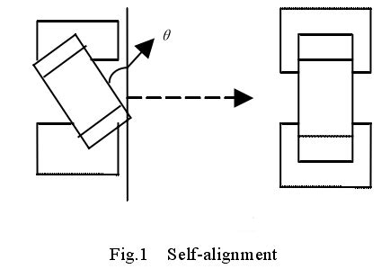
Tombstoning, a critical defect in PCB assembly, occurs when surface-mount components lift vertically during reflow soldering, compromising electrical connections. To address this in PCBA manufacturing, engineers focus on balancing forces acting on components through design and process optimizations. A primary strategy involves refining pad geometry to ensure symmetrical solder wetting. For instance, reducing pad size discrepancies between component terminals minimizes uneven surface tension, a key contributor to tombstoning.
Thermal management also plays a pivotal role. Uneven heating across the board creates thermal gradients, causing one end of a component to reflow faster than the other. By calibrating oven zones to achieve gradual temperature ramps and uniform heat distribution, manufacturers mitigate this imbalance. Additionally, precise solder paste application—using laser-cut stencils with optimized aperture ratios—ensures consistent volume deposition. This prevents one pad from generating excessive molten solder, which could otherwise "pull" the component upward.
Component alignment accuracy further reduces risks. Automated optical inspection (AOI) systems verify placement tolerances, while pick-and-place machines with enhanced calibration capabilities minimize positional errors. Integrating these measures into PCBA workflows not only addresses tombstoning but also enhances overall process reliability, reducing rework costs and improving yield rates in high-volume production.
Optimizing PCB Pad Layouts to Avoid Tombstoning
Effective PCB assembly relies on precise pad design to prevent tombstoning—a defect where surface-mount components partially lift during reflow soldering. Central to mitigation is ensuring thermal mass balance between paired pads. Asymmetric pad geometries create uneven heat distribution, causing one end of a component to solidify faster than the other. To address this, designers should prioritize symmetrical pad dimensions and consistent spacing from component terminals. For example, elongated pads for passive components like resistors or capacitors can reduce tension imbalances during solder solidification.
In PCBA processes, pad orientation also plays a critical role. Aligning pads perpendicular to the reflow oven’s airflow direction minimizes localized cooling disparities. Additionally, incorporating thermal relief connections in ground or power planes helps regulate heat transfer, preventing rapid temperature fluctuations at specific pads. Design software tools now include automated checks for pad-to-component ratio mismatches, flagging high-risk layouts before manufacturing.
A common oversight involves neglecting pad surface finishes. Using immersion silver or ENIG (Electroless Nickel Immersion Gold) coatings ensures uniform solder wetting, reducing the likelihood of uneven adhesion. For fine-pitch components, micro-via pad structures can further enhance mechanical stability. By integrating these strategies into PCB assembly workflows, manufacturers significantly lower defect rates while maintaining alignment with industry standards like IPC-7351 for land pattern design.

Thermal Profile Adjustments for Tombstone Prevention
Precise control of thermal gradients during PCB assembly remains a critical factor in mitigating tombstoning defects. Uneven heating across surface-mount components creates differential solder wetting forces, which can lift one end of a device before the other fully adheres. To address this, engineers optimize reflow oven profiles by balancing ramp rates, soak times, and peak temperatures. A gradual preheat phase (1–3°C/second) minimizes thermal shock, while extended soak zones ensure uniform heat distribution across PCBA substrates. For temperature-sensitive components like MLCCs or chip resistors, reducing peak reflow temperatures by 5–10°C can prevent premature solder solidification on one terminal.
Additionally, symmetrical component placement relative to board edges or heat sinks helps equalize thermal mass distribution. Real-time monitoring systems track thermocouple data to validate profile consistency, particularly for mixed-technology boards with both large and miniature components. When paired with optimized pad designs and solder paste deposition, these thermal adjustments reduce wetting imbalance—a primary driver of tombstoning. Manufacturers often conduct design of experiments (DOE) to identify ideal profile parameters for specific PCBA configurations, ensuring repeatable results across production batches. By aligning thermal management with material properties and device geometries, assembly teams achieve higher yields while maintaining reliability in high-density electronic systems.
Solder Paste Application Techniques to Reduce Tombstoning
Precise solder paste application forms the foundation of reliable PCB assembly processes, directly influencing tombstoning risks in surface-mount technology (SMT). In PCBA manufacturing, uneven solder paste deposition creates imbalanced wetting forces during reflow, which can lift one end of a component. To mitigate this, engineers prioritize stencil design optimization, ensuring aperture geometry matches component pad dimensions. For smaller components like 0201 or 01005 resistors, reduced stencil thickness (e.g., 100–120 μm) paired with laser-cut apertures improves paste release consistency.
Controlled solder paste volume is equally critical. Excessive paste increases surface tension differentials, while insufficient material fails to anchor components. Automated paste inspection (SPI) systems validate deposition accuracy, flagging deviations exceeding ±10% of target volume. Additionally, solder paste viscosity must align with printing speeds—higher viscosity pastes resist slumping but require precise squeegee pressure adjustments.
Selecting solder alloys with appropriate wetting properties further reduces tombstoning. For example, SAC305 (Sn96.5/Ag3.0/Cu0.5) offers balanced thermal and mechanical stability compared to high-silver alternatives, which may exacerbate uneven melting. Integrating nitrogen-assisted reflow environments minimizes oxidation, promoting uniform solder flow.
Finally, process controls like regular stencil cleaning and printer calibration ensure repeatability. By harmonizing these techniques, PCB assembly teams achieve defect rates below 0.1%, aligning with IPC-A-610 standards for SMT reliability.
Key Factors in Tombstoning Prevention During Reflow
Controlling thermal dynamics and solder behavior during reflow soldering remains critical for preventing tombstoning in PCB assembly. Uneven heating across component terminals creates imbalanced surface tension, which lifts one end of the device. To address this, engineers must optimize thermal profiles to ensure symmetrical heat distribution. This involves balancing ramp rates, peak temperatures, and time above liquidus (TAL) across all PCBA pads. For instance, reducing the temperature gradient between larger and smaller pads minimizes differential solder solidification rates.
Additionally, solder paste volume and composition play pivotal roles. Insufficient paste on one pad can lead to premature melting, while excessive deposition may cause floating components. Modern PCB assembly lines employ precision stencil designs and automated inspection systems to maintain consistent paste deposition. Pairing this with nitrogen-enriched reflow environments reduces oxidation, enhancing wetting uniformity.
Finally, component alignment accuracy during placement ensures balanced contact with solder paste. Even minor misalignments can amplify thermal imbalances during reflow. Advanced pick-and-place systems with vision-guided calibration are now standard in high-reliability PCBA production, effectively mitigating this risk. By integrating these strategies, manufacturers achieve stable solder joint formation while minimizing tombstoning defects.
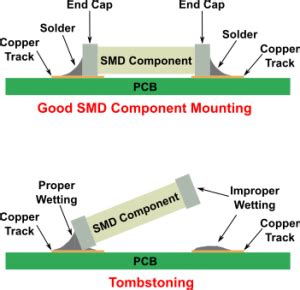
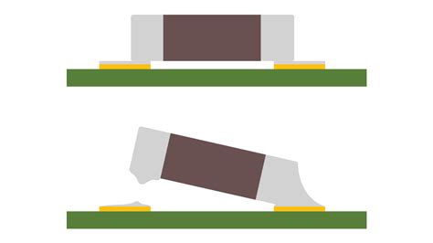
Understanding Root Causes of Tombstoning Defects
Tombstoning defects in PCB assembly occur when one end of a surface-mount component lifts during reflow soldering, creating an open circuit. This phenomenon primarily stems from imbalanced forces acting on the component terminals. Key contributors include thermal gradients across the PCBA, uneven solder paste deposition, and asymmetrical pad geometries.
| Root Cause | Mechanism | Impact on Tombstoning |
|---|---|---|
| Thermal Imbalance | Differential heating/cooling rates | Uneven solder melt/solidification |
| Pad Design Flaws | Mismatched pad sizes or shapes | Asymmetric surface tension forces |
| Solder Paste Issues | Inconsistent volume or alignment | Variable wetting behavior |
Thermal mismatches often arise from improper reflow oven profiles, where rapid temperature changes create unequal molten solder cohesion. For example, smaller components like 0201 resistors are more susceptible due to their lower mass. Similarly, pad layouts with disproportionate surface areas amplify surface tension differentials, pulling components toward the larger pad. In PCBA processes, solder paste stencil apertures must align precisely with pads to ensure uniform deposition – even minor misalignments can trigger tombstoning. By analyzing these root causes, manufacturers can implement targeted corrections, such as optimizing pad symmetry or refining thermal ramp rates, to minimize defect rates in high-density assemblies.
Best Practices for SMT Component Alignment
Proper alignment of SMT components during PCB assembly is critical for minimizing tombstoning defects. Component misalignment creates uneven thermal and mechanical forces during reflow, increasing the risk of one end lifting from the pad. To ensure precision, manufacturers should leverage automated optical inspection (AOI) systems to verify placement accuracy before reflow. These systems detect angular offsets or positional deviations as small as 0.05mm, enabling real-time corrections.
Designers must also prioritize pad geometry symmetry in PCBA layouts. For passive components like resistors or capacitors, rectangular pads should maintain identical dimensions and spacing to balance solder wetting forces. Additionally, aligning components parallel to the board’s primary reflow direction reduces uneven heating, which can exacerbate tombstoning. When placing smaller components (e.g., 0201 or 0402 packages), ensure feeders in pick-and-place machines are calibrated to prevent skewed placements.
A controlled placement speed further enhances alignment consistency. High-speed machines may sacrifice precision, particularly for miniaturized components. Pairing slower placement rates with vacuum nozzles sized to component dimensions minimizes positional shifts. Finally, verifying stencil alignment with fiducial markers ensures solder paste deposits align perfectly with pads, creating a uniform foundation for component anchoring. These practices, integrated into the PCB assembly workflow, significantly reduce tombstoning risks while maintaining throughput efficiency.
Comprehensive Strategies for Tombstoning Mitigation
Effective tombstoning prevention in PCB assembly requires a holistic approach that integrates design, process, and material considerations. While optimizing pad layouts and refining thermal profiles form the foundation, advanced PCBA workflows demand additional safeguards. Combining multiple technical interventions—such as balanced solder paste deposition and symmetrical component placement—ensures uniform wetting forces during reflow, counteracting the uneven torque that lifts components.
Critical elements include implementing dynamic stencil designs to regulate paste volume across pads and adopting low-temperature solder alloys to minimize thermal gradients. For high-density boards, pairing automated optical inspection (AOI) with real-time process monitoring helps detect early signs of misalignment before reflow. Additionally, calibrating pick-and-place machines to account for component mass disparities reduces mechanical imbalances during placement.
Material selection also plays a pivotal role: using solder pastes with tailored viscosity profiles improves cohesion, while substrate materials with matched coefficients of thermal expansion (CTE) prevent differential warping. By synchronizing these strategies, manufacturers achieve defect rates below 0.5% in high-volume PCB assembly lines, even with miniaturized components. This systematic integration of design precision, process control, and material science establishes robust safeguards against tombstoning across diverse PCBA applications.
Conclusion
Effective prevention of tombstoning in PCB assembly requires a holistic approach that integrates design, process control, and material optimization. By prioritizing pad geometry symmetry and balanced thermal mass distribution during layout design, manufacturers can minimize uneven solder wetting forces that lead to component lifting. Equally critical is refining reflow oven profiles to reduce thermal gradients across PCBA substrates, ensuring uniform heating and cooling rates.
Modern PCB assembly lines benefit from advanced solder paste stenciling techniques, such as stepped apertures or optimized deposition volumes, which prevent skewed component floatation during reflow. Pairing these methods with real-time pick-and-place alignment verification further reduces misregistration risks. While no single solution guarantees absolute elimination of tombstoning, combining preventive design principles with rigorous process monitoring creates a robust defense against this defect.
As miniaturization trends push component sizes below 0402 metrics, the interplay between material selection (e.g., low-agitation solder alloys) and equipment precision becomes increasingly vital. By adopting these strategies, PCBA manufacturers can achieve higher first-pass yields while maintaining the structural integrity of surface-mount interconnections in demanding applications.
FAQs
What causes tombstoning defects in PCB assembly?
Tombstoning occurs when uneven forces during reflow soldering lift one end of a surface-mount component. Common causes include mismatched pad thermal mass, uneven solder paste application, or rapid temperature gradients across the component.
How does pad design optimization reduce tombstoning risks in PCBA?
Symmetrical pad layouts ensure balanced heat distribution, minimizing differential melting of solder. Incorporating thermal relief patterns and matching pad sizes to component terminals also stabilizes alignment during reflow.
Can solder paste stencil design impact tombstoning prevention?
Yes. Precision stencil apertures control solder paste volume, ensuring consistent deposition. Reduced paste volume on smaller pads prevents excessive pull forces, while proper viscosity maintains print definition before reflow.
Why is thermal profiling critical for preventing tombstoning?
A gradual ramp-to-peak profile reduces thermal shock, allowing even solder melting. Balancing zone temperatures across the PCB assembly prevents localized hotspots that could destabilize components.
How do automated inspection systems help mitigate tombstoning?
Vision systems detect misaligned components or uneven paste deposition before reflow, enabling corrections. Post-reflow AOI identifies early-stage defects, supporting process adjustments in PCBA workflows.
Optimize Your Next PCB Assembly Project
For tailored solutions to combat tombstoning and enhance manufacturing reliability, please click here to consult our PCBA experts.