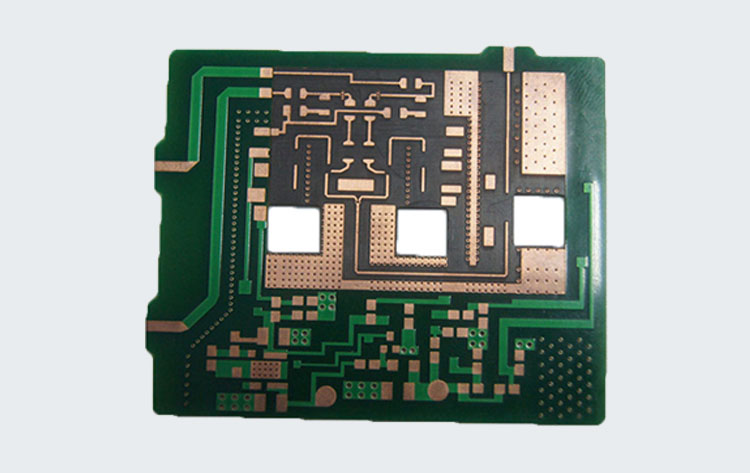
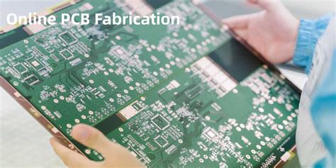
Efficient Online PCB Manufacturing for Rapid Prototyping
Key Takeaways
When exploring PCB manufacturing for prototyping, understanding core advantages can significantly impact your project’s success. Modern PCB manufacturing companies leverage digital tools to streamline workflows, allowing you to upload designs, receive instant online quotes, and track production in real time. This eliminates traditional delays, ensuring faster iterations and reduced PCB manufacturing cost through automated error detection and material optimization.
A critical advantage lies in global shipping networks, which enable seamless delivery of prototypes regardless of your location. Combined with rapid turnaround methods—such as automated assembly lines and advanced etching techniques—these services compress timelines from weeks to days. For businesses managing tight deadlines, this efficiency is invaluable, particularly when scaling a PCB manufacturing business or testing product-market fit.
Online platforms also simplify collaboration with engineers via 24/5 chat support, offering clarity on design specifications or material choices. This real-time guidance helps avoid costly revisions. Additionally, integrating precision engineering ensures consistency across batches, whether you’re producing 10 or 10,000 units.
By partnering with a trusted provider like Andwin PCB, you gain access to end-to-end solutions that balance speed, accuracy, and affordability. From initial prototyping to full-scale production, these services empower you to focus on innovation while minimizing logistical hurdles—a strategic edge in today’s fast-paced electronics landscape.
/5 PCB Prototyping Services Explained
When exploring PCB manufacturing for prototyping, understanding the five core service pillars helps streamline your project’s path from concept to physical board. Modern online platforms simplify this process by integrating design validation, instant quoting, material selection, production scheduling, and delivery coordination into a unified workflow.
The journey typically begins with uploading your design files, where automated tools check for critical errors like trace spacing or layer misalignment. This step ensures your design meets the pcb manufacturing companies’ fabrication standards before moving forward. Once validated, you’ll receive an instant quote that breaks down pcb manufacturing cost factors—board size, layer count, and material choices like FR-4 or high-frequency substrates. For startups, this transparency is vital for budgeting iterative prototypes.
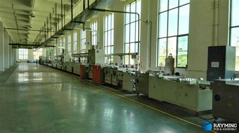
Next, production timelines come into focus. Many services offer rapid turnaround options—as fast as 24 hours—for simple designs, ideal for design verification phases. Advanced methods like automated optical inspection (AOI) and flying probe testing are often included, ensuring reliability without inflating costs. For businesses scaling a pcb manufacturing business, these quality controls reduce post-production troubleshooting.
Finally, global logistics integrations ensure boards reach your lab or facility efficiently. Coupled with 24/5 chat support, this end-to-end approach minimizes delays and keeps projects on track. Whether you’re testing a new IoT sensor or refining a medical device, leveraging these five service layers accelerates development while maintaining precision—a balance critical in competitive tech markets.
Instant Online Quotes for Circuit Boards
Securing real-time pricing for PCB manufacturing projects has become a cornerstone of modern prototyping workflows. Leading PCB manufacturing companies now integrate automated quotation systems that analyze design files within minutes, eliminating days of manual back-and-forth. By uploading Gerber files or CAD designs directly to a supplier’s portal, you receive a PCB manufacturing cost breakdown that factors in board dimensions, layer counts, material grades, and surface finishes—all without human intervention.
This shift toward digitized quoting aligns with the demands of today’s PCB manufacturing business, where speed and transparency directly impact product development cycles. Advanced algorithms cross-reference your specifications with production capacity and material availability, offering dynamic pricing even for complex designs like HDI or flexible circuits. For time-sensitive projects, some platforms highlight cost-saving alternatives—such as adjusting panelization layouts or opting for lead-free HASL finishes—to help balance quality and budget.
While evaluating quotes, consider how global logistics and turnaround timelines affect total expenses. Reputable providers often bundle shipping estimates into initial quotes, letting you compare regional and international PCB manufacturing companies side by side. To further streamline decision-making, look for platforms that retain your project history, enabling repeat orders with pre-validated parameters. This not only accelerates future prototyping but also builds a predictable cost framework for scaling production.
The ability to instantly gauge PCB manufacturing cost transforms how teams allocate resources, particularly when iterating designs under tight deadlines. By reducing quotation delays from weeks to minutes, these systems empower engineers to focus on innovation rather than administrative overhead—a critical advantage in competitive hardware markets.
Global Shipping for PCB Manufacturing
When selecting PCB manufacturing companies for your projects, global shipping capabilities are a critical factor in ensuring timely delivery and cost efficiency. Modern online PCB manufacturing platforms leverage established logistics networks to deliver prototypes and production-grade boards worldwide, often consolidating orders to optimize PCB manufacturing cost. This eliminates the geographic constraints traditionally associated with circuit board production, allowing startups and enterprises alike to collaborate with specialized suppliers regardless of location.
Leading providers integrate real-time shipping calculators into their quoting systems, enabling you to preview delivery timelines and fees before finalizing orders. For time-sensitive projects, expedited air freight options—paired with rapid turnaround PCB production methods—ensure components reach your facility within 3–5 business days. Meanwhile, consolidated sea freight becomes cost-effective for bulk orders, reducing per-unit expenses in high-volume PCB manufacturing business operations.
Regional compliance is another advantage of working with globally connected partners. Reputable manufacturers pre-certify boards for international standards like CE, FCC, and RoHS, minimizing customs delays. Some even offer localized warehousing to enable regional inventory distribution, further accelerating restocking cycles.
To maximize value, compare how different PCB manufacturing companies structure their shipping policies. Look for transparent pricing models that bundle duties and taxes, avoiding hidden surcharges. Additionally, verify carrier partnerships—established collaborations with DHL, FedEx, or UPS often translate to reliable tracking and reduced transit risks.
By prioritizing global logistics capabilities in your supplier selection, you transform geographical diversity from a challenge into a strategic asset. Whether scaling production across continents or iterating prototypes with overseas engineering teams, seamless shipping integration ensures your PCB manufacturing workflow remains uninterrupted and cost-competitive.

Rapid Turnaround PCB Production Methods
To meet tight deadlines without compromising quality, modern PCB manufacturing relies on advanced methodologies that prioritize speed at every stage. Leading PCB manufacturing companies leverage automated design verification tools to eliminate manual errors, reducing pre-production delays by up to 70%. For instance, AI-driven DFM (Design for Manufacturability) checks instantly flag issues like insufficient trace spacing, allowing you to revise files in real time before fabrication begins.
A critical factor in accelerating production is optimizing material selection. While PCB manufacturing cost often correlates with substrate quality, high-speed laminates like FR-4 HTG balance performance and affordability for prototyping. Here’s how traditional and rapid methods compare:
| Factor | Traditional PCB Production | Rapid Turnaround Services |
|---|---|---|
| Lead Time | 10–15 business days | 24–72 hours |
| Order Flexibility | Minimum 50 boards | 1–10 prototypes |
| Cost per Unit | $8–$15 | $12–$25 |
| Revision Cycle | 3–5 days | <24 hours |
By partnering with a PCB manufacturing business specializing in express services, you gain access to parallel processing workflows. Multiple production stages—like drilling, plating, and solder mask application—occur simultaneously across dedicated equipment lines. This approach slashes turnaround times by 40% compared to sequential manufacturing.
To further streamline timelines, many providers offer modular pricing: pay only for essential services like basic testing or surface finishes. For example, skipping gold plating on non-critical connectors can reduce both PCB manufacturing cost and processing time by 15%. However, always verify whether accelerated timelines align with your quality standards—some rapid methods may limit layer counts or minimum trace widths.
Advanced logistics integration also plays a role. Same-day shipping partnerships and regional fulfillment centers enable PCB manufacturing companies to guarantee delivery within 96 hours, even for international orders. This eliminates bottlenecks between production completion and physical prototyping, ensuring you receive boards while design iterations are still fresh.
Streamlining Prototyping with Online Tools
Modern PCB manufacturing workflows thrive on digital efficiency, and leveraging online tools can transform how you approach prototyping. By integrating cloud-based platforms, PCB manufacturing companies enable engineers to upload designs, receive instant feedback, and track production progress in real time—all without leaving their workspace. These tools often include automated design rule checks (DRC) to flag potential issues early, reducing costly revisions and accelerating time-to-market.
"Adopting online collaboration tools cuts PCB manufacturing cost by minimizing communication gaps and ensuring design specifications are met before production begins."
When evaluating platforms, prioritize those offering version control and multi-user access to streamline team collaboration. Many services now feature interactive dashboards that visualize PCB manufacturing business metrics, such as material costs and lead times, allowing you to adjust designs for budget or timeline constraints. For instance, swapping substrate materials or adjusting layer counts can be simulated instantly to compare cost-impact scenarios.
Advanced tools also integrate with component libraries, automatically checking part availability across global suppliers. This prevents delays caused by last-minute substitutions and ensures your prototype aligns with mass production requirements. Additionally, some platforms offer AI-driven suggestions for optimizing trace layouts or thermal management—critical for high-performance boards.
By centralizing design, quoting, and ordering processes, these solutions eliminate the back-and-forth traditionally associated with prototyping. You’re no longer waiting days for email responses; instead, automated notifications keep you informed at every stage, from panelization to shipping. This transparency not only reduces PCB manufacturing cost but also builds trust with your chosen PCB manufacturing companies, fostering long-term partnerships.
Transitioning to digital tools does require upfront familiarization, but the payoff in speed and precision is undeniable. Start with free trials or demo accounts to test compatibility with your workflow before committing. Remember, the goal isn’t just faster prototypes—it’s creating a repeatable, scalable process that aligns with your PCB manufacturing business goals.
Precision Engineering for PCB Manufacturing
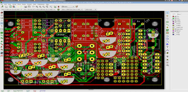
When developing electronic products, the reliability of your PCB manufacturing process hinges on precision engineering principles. Modern PCB manufacturing companies leverage advanced technologies like laser direct imaging (LDI) and automated optical inspection (AOI) to achieve tolerances as tight as ±0.002 inches. These systems ensure that even high-density interconnect (HDI) designs with microvias and fine-pitch components meet exact specifications.
Material selection plays a critical role here. For instance, choosing between FR-4, Rogers, or polyimide substrates directly impacts thermal stability and signal integrity—factors that affect both performance and long-term PCB manufacturing cost. Advanced firms optimize layer stack-ups using simulation tools to minimize impedance mismatches, reducing the risk of post-production revisions.
In the PCB manufacturing business, balancing speed with accuracy is non-negotiable. While rapid prototyping demands quick turnarounds, precision ensures that your boards function correctly on the first iteration. Techniques like controlled-depth drilling and solder mask application via liquid photo imaging (LPI) prevent defects such as copper voids or mask misalignment, which could delay product launches.
Transitioning from design to production, automated file validation checks in online platforms help you avoid common errors like insufficient clearance or missing drill files. This seamless integration between engineering and manufacturing workflows allows you to focus on innovation rather than troubleshooting. By prioritizing precision at every stage, you not only safeguard product quality but also streamline scalability—a decisive advantage in competitive markets.
Chat Support in PCB Manufacturing Services
When navigating PCB manufacturing processes, real-time communication bridges the gap between technical requirements and production execution. Modern PCB manufacturing companies integrate live chat support to address design ambiguities, material selection, and PCB manufacturing cost optimization without delaying project timelines. Imagine finalizing a prototype design at midnight—with 24/5 chat access, you can instantly clarify solder mask specifications or validate layer stack-up configurations, ensuring your files meet fabrication guidelines before submission.
This becomes particularly valuable when balancing quality and budget. For instance, chat agents can recommend cost-effective substrate materials or suggest panelization strategies to minimize waste—critical factors for startups managing tight PCB manufacturing business margins. They might also explain how design complexity impacts pricing, helping you decide whether to reduce via counts or adjust trace widths. Proactively resolving these questions prevents costly revisions and accelerates order approvals.
Moreover, chat logs create an audit trail for future reference, streamlining repeat orders or scaling production. If you’re coordinating with global teams, instant messaging ensures all stakeholders stay aligned on changes, from impedance control requirements to delivery timelines. For time-sensitive projects, this immediacy complements rapid turnaround services, allowing you to troubleshoot Gerber file issues while the production line is still active.
By embedding chat support into their workflows, PCB manufacturing providers transform a traditionally opaque process into a collaborative experience. Whether you’re optimizing PCB manufacturing cost or exploring advanced HDI board options, having experts just a message away adds a layer of precision to prototyping—and peace of mind for your product development cycle.
Accelerating Product Development with PCBs
When bringing a new electronic product to market, time-to-market is often the difference between success and obsolescence. This is where partnering with PCB manufacturing companies that specialize in rapid prototyping becomes critical. By leveraging online platforms, you can submit design files and receive instant quotes for PCB manufacturing cost within minutes, eliminating the delays of traditional RFQ processes. Modern PCB manufacturing business models prioritize agility, offering design-for-manufacturability (DFM) feedback directly through automated systems to help refine your boards before production begins.
The integration of cloud-based collaboration tools allows engineering teams to iterate designs in real time, synchronizing revisions across global stakeholders. For hardware startups, this means compressing weeks of back-and-forth communication into days. Advanced PCB manufacturing services further accelerate development by supporting mixed-technology assemblies—combining rigid, flexible, and HDI boards in a single order—which simplifies testing complex systems.
Cost predictability also plays a pivotal role in speeding up cycles. Transparent PCB manufacturing cost structures let you allocate budgets more effectively, reducing financial uncertainty during iterative prototyping phases. Meanwhile, scalable production capabilities ensure that validated designs can transition seamlessly from low-volume batches to mass manufacturing without requalifying suppliers.
By aligning with PCB manufacturing companies that offer end-to-end digital workflows, you eliminate bottlenecks in sourcing, quality checks, and logistics. Real-time order tracking and automated documentation further streamline compliance, freeing engineers to focus on innovation rather than administrative tasks. In industries where every day counts, this operational efficiency transforms PCB manufacturing from a logistical hurdle into a strategic accelerator.
Conclusion
When navigating the complexities of PCB manufacturing, the shift toward digital solutions has fundamentally transformed how businesses approach prototyping. By partnering with specialized PCB manufacturing companies, you gain access to advanced tools that simplify design validation, material selection, and cost optimization—all while maintaining tight control over PCB manufacturing cost. Modern platforms enable real-time collaboration, automated error detection, and transparent pricing models, ensuring your PCB manufacturing business stays competitive in fast-paced markets.
The integration of cloud-based quoting systems and AI-driven analytics reduces delays traditionally associated with manual processes, allowing you to focus on iterative improvements rather than logistical hurdles. Whether you’re refining a high-frequency circuit or scaling production for IoT devices, the ability to instantly adjust designs and receive global shipping updates ensures time-to-market advantages.
As industries demand faster innovation cycles, leveraging these digital frameworks becomes less optional and more strategic. The right balance of precision engineering and agile workflows not only safeguards product quality but also aligns with evolving customer expectations. By prioritizing efficiency in PCB manufacturing, you position your projects to thrive in an era where speed and reliability define success.
FAQs
How does online PCB manufacturing streamline prototyping?
By leveraging automated quoting systems and real-time design verification, PCB manufacturing services eliminate manual back-and-forth. You receive instant feedback on design feasibility, material options, and PCB manufacturing cost estimates, reducing pre-production delays.
What factors influence PCB manufacturing costs?
Cost depends on board complexity, layer count, material type, and turnaround time. Many PCB manufacturing companies offer tiered pricing—opting for standard materials or slightly longer lead times can lower expenses without compromising quality.
How do I choose reliable PCB manufacturing companies?
Prioritize providers with ISO certifications, transparent PCB manufacturing business practices, and verified customer reviews. Look for firms offering 24/7 chat support and detailed documentation, such as Gerber file guidelines and testing protocols.
Can online tools accelerate PCB production timelines?
Yes. Integrated platforms allow you to upload designs, analyze manufacturability, and approve quotes within hours. Some services even pair automated workflows with global shipping networks to deliver prototypes in as few as 24 hours.
What advantages do online PCB manufacturing businesses offer startups?
They provide scalable solutions—order small batches for testing, then ramp up production seamlessly. Many platforms also offer design-for-manufacturing (DFM) reports, helping you avoid costly errors before committing to full-scale PCB manufacturing.
Ready to Start Your PCB Project?
For instant quotes and expert guidance tailored to your prototyping needs, please click here to explore https://www.andwinpcb.com/pcb-manufacturing/.