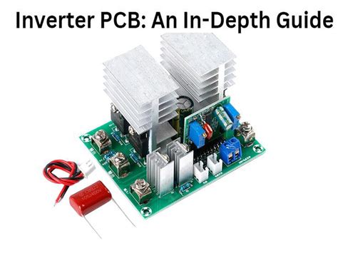
Efficient PCB Assembly Solutions for Inverter Technologies
Key Takeaways
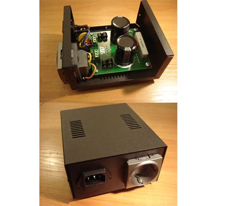
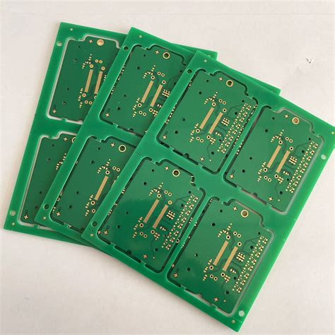
Efficient PCB assembly is vital for the performance and reliability of inverter technologies. The way in which PCBA is executed can significantly affect the overall effectiveness of energy conversion systems. By employing state-of-the-art techniques and materials, manufacturers can enhance the efficiency of their inverter products. Recent advancements in pcb assembly methods, such as surface mount technology (SMT) and through-hole technology, allow for more compact designs and better thermal management. Key materials like high-frequency laminates and thermal conductive substrates are essential for high-performance PCBA, enabling more robust energy conversions.
In implementing these solutions, companies should adopt best practices to ensure the reliability of their inverter assemblies. This includes rigorous testing protocols, proper handling procedures, and implementing quality control measures throughout the production process to mitigate any potential issues.
“Investing in quality PCB assembly processes now can pave the way for greater efficiency and reliability in the future,” suggests an industry expert.
To illustrate the importance of selecting the right components and materials during pcb assembly, consider the following table:
| Material | Properties | Application in Inverters |
|---|---|---|
| FR-4 | Insulating with good strength | Standard PCBs |
| Rogers 4350B | High-frequency capabilities | RF and microwave applications |
| Aluminum Oxide | Excellent thermal conductivity | Cooling solutions for components |
By focusing on these key elements of pcba, manufacturers can not only improve their current offerings but also prepare to meet future demands in a rapidly evolving technological landscape.
Introduction to Inverter Technologies and PCB Assembly
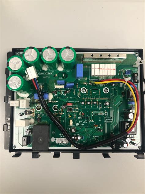
In recent years, inverter technologies have become increasingly critical in various applications, particularly within renewable energy systems such as solar and wind power. At the heart of any inverter system is the Printed Circuit Board Assembly (PCBA), which serves as the foundational framework for integrating multiple electronic components. Efficient pcb assembly is paramount for ensuring that these devices operate reliably and effectively, as they are responsible for converting direct current (DC) into alternating current (AC). The integration of high-quality materials and advanced manufacturing processes plays a significant role in enhancing the performance of these systems. A well-executed pcb assembly not only minimizes signal loss but also contributes to reducing thermal issues and increasing overall efficiency. As such, the relationship between inverter technologies and pcba techniques is intrinsic; advancements in assembly practices directly impact the robustness and longevity of inverter systems, making it essential to prioritize innovative solutions that address both performance and reliability in energy conversion applications.
Importance of Efficient PCB Assembly in Energy Conversion
Efficient PCB assembly is pivotal in the realm of energy conversion, particularly for inverter technologies. The effectiveness of pcba directly influences the performance and durability of energy systems, making it essential to adopt superior assembly techniques. Inverter systems play a vital role in transforming direct current (DC) into alternating current (AC), and the reliability of these applications heavily relies on quality PCB assembly practices. A well-executed pcba can minimize losses and enhance overall efficiency, which is crucial for applications such as renewable energy systems and electric vehicles. Moreover, with advancements in technology, employing innovative methods during the PCB assembly process can lead to substantial improvements in thermal management and signal integrity, both critical for successful operation. By focusing on precise component placement and soldering quality, manufacturers can ensure that their inverter technologies not only function optimally but also withstand various environmental stresses over time. In summary, the significance of efficient pcb assembly cannot be understated as it forms the backbone of reliable energy conversion systems that are becoming increasingly relevant in today’s energy landscape.
Latest Methods in PCB Assembly for Inverters
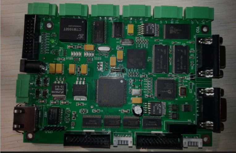
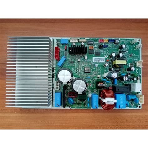
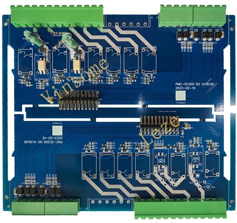
As the demand for efficient inverter technologies continues to grow, advancements in pcb assembly methods have become crucial. Recent trends emphasize the integration of advanced automation processes, such as pick and place machines and robotic soldering, which enhance precision and speed in pcba production. These techniques not only reduce the likelihood of human error but also ensure a higher level of consistency, resulting in more reliable energy conversion systems. Additionally, the adoption of surface mount technology (SMT) has streamlined the assembly process, allowing for more compact designs that can maximize space and efficiency within inverter units. Furthermore, innovative bonding methods, such as low-temperature soldering and conductive adhesives, are gaining traction as they not only improve thermal management but also support the assembly of sensitive components without damage. With a focus on sustainability, many manufacturers are also incorporating environmentally friendly materials into their pcb assemblies, responding to a stronger push towards greener technologies. These latest methods collectively contribute to a more efficient and reliable approach to pcb assembly, which is essential in optimizing the performance of modern inverter systems.
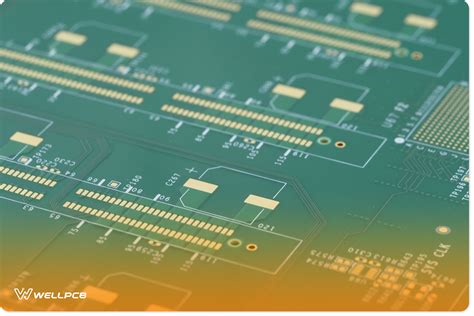
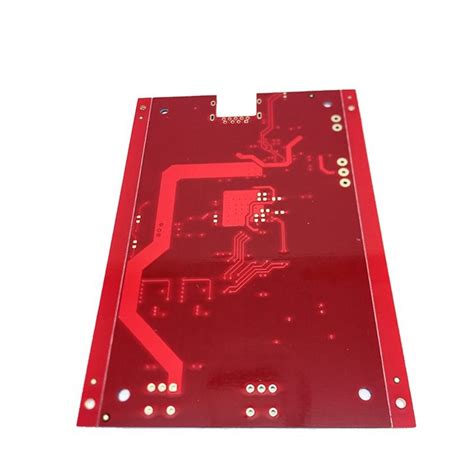
Key Materials for High-Performance PCB Assemblies
In the realm of pcb assembly for inverter technologies, the selection of materials is pivotal to ensuring optimal performance and reliability. Key materials often employed in pcba include advanced substrates, which provide excellent thermal stability and electrical insulation. For instance, FR-4 epoxy resin is commonly used due to its balance of affordability and performance, while high-frequency laminates made from materials such as PTFE are essential for applications requiring superior signal integrity. Furthermore, incorporating copper with varying thickness can significantly impact the thermal management capabilities of the assembly, ensuring efficient heat dissipation during operation. Additionally, solder masks and surface finishes like HASL (Hot Air Solder Leveling) or ENIG (Electroless Nickel/Immersion Gold) are crucial for enhancing solder reliability and preventing oxidation. Using these high-grade materials not only bolsters the functionality of the inverter systems but also contributes to longer operational lifespans, showcasing how thoughtful material selection in pcb assembly can directly influence overall energy conversion efficiency.
Best Practices in PCB Assembly for Enhanced Reliability
In the realm of inverter technologies, achieving optimal reliability in the PCB assembly (PCBA) process is paramount. One of the best practices involves ensuring meticulous design reviews prior to assembly. This includes assessing layout designs to eliminate potential issues such as signal integrity problems and thermal management failures, which can severely impact performance. Additionally, selecting high-quality materials tailored for specific applications can markedly increase reliability. For instance, using FR-4 materials with optimal dielectric properties supports better thermal and electrical performance in energy conversion systems. Furthermore, adopting automated PCBA processes enhances precision and consistency, reducing the chances of human error during assembly. Implementing effective soldering techniques, such as using lead-free solder, can also contribute to a more reliable product lifecycle. Testing methods such as in-circuit testing (ICT) and functional testing must be employed rigorously throughout the manufacturing phase to identify potential defects early on. By adhering to these best practices, manufacturers can significantly enhance the durability and efficacy of their inverter systems while ensuring that their investment yields long-term dividence in both performance and reliability.
Challenges and Solutions in PCB Assembly for Inverter Systems
The pcb assembly process for inverter systems presents a myriad of challenges that can impact the overall performance and reliability of these critical components in energy conversion applications. One prominent challenge is managing the increasing complexity of modern inverter designs, which often incorporate various technologies and require meticulous attention to detail during the pcba process. This complexity can lead to issues such as thermal management, signal integrity, and component placement, all of which are vital for optimizing performance. To address these challenges, manufacturers are increasingly adopting advanced pcb assembly techniques that include automated component placement and inspection technologies. These methods not only streamline the assembly process but also ensure higher precision and reduced errors.
Additionally, the selection of appropriate materials is crucial in overcoming these challenges. High-quality substrates with excellent thermal conductivity are essential to manage heat dissipation effectively, while reliable solder materials ensure robust connections that withstand operational stress. Companies are also focusing on implementing rigorous testing protocols throughout the pcba process to identify potential failures early on. By integrating feedback loops into production lines, any discrepancies can be rectified promptly, ensuring that only high-quality inverter assemblies reach the market. Ultimately, facing these challenges head-on with innovative solutions enhances both the performance and longevity of inverter systems, making them more reliable in various applications across the energy sector.
Future Trends in PCB Assembly Technologies for Inverters
The future trends in PCB assembly technologies for inverter systems are being shaped by advancements in both materials and processes that aim to improve the efficiency and reliability of energy conversion systems. One notable trend is the increased integration of automated processes which enhance precision and reduce production time for printed circuit board assemblies (PCBA). As inverter applications demand more complex designs, the use of high-density interconnect (HDI) techniques in pcb assembly is becoming commonplace. These techniques not only optimize space but also improve electrical performance, enabling smaller and more efficient inverter designs.
Moreover, the adoption of lead-free soldering practices is on the rise, aligning with environmental standards and pushing manufacturers toward sustainable solutions. The employment of advanced materials, such as thermally conductive substrates, is also expected to play a crucial role in managing heat dissipation within inverters, ensuring longevity and stability under varying operational conditions. Furthermore, ongoing research into flexible PCB technologies could allow for greater design versatility, paving the way for innovative inverter configurations.
Overall, these trends indicate a shift towards more sustainable practices, enhanced performance capabilities, and increased customization options in the realm of pcb assembly for inverter technologies. As these advancements continue to evolve, they will undoubtedly influence industry standards and set new benchmarks for reliability and efficiency in energy conversion systems.
Conclusion
In summary, the landscape of pcb assembly for inverter technologies is continuously evolving, driven by the need for higher efficiency and reliability in energy conversion systems. As we have explored throughout this article, implementing advanced techniques in pcba plays a pivotal role in optimizing the performance of inverters. The integration of modern materials enhances the durability and functionality of assemblies, addressing critical demands within this field. Moreover, adhering to best practices ensures that manufacturers can overcome common challenges faced during pcb assembly processes. Looking forward, staying abreast of emerging trends and innovations will be essential for sustaining advancements in inverter technologies. Overall, effective pcba is not just a technical necessity but a cornerstone for the future of sustainable energy solutions.
FAQs
What is PCB assembly in inverter technologies?
PCB assembly (PCBA) in inverter technologies refers to the process of assembling various electronic components onto a printed circuit board (PCB) specifically designed for inverters. This assembly plays a critical role in ensuring efficient energy conversion.
Why is efficient PCB assembly important for inverter performance?
An efficient pcb assembly enhances the overall performance of inverter systems by ensuring the reliable connection and functionality of all components, thus optimizing energy conversion and minimizing losses during operation.
What are some common methods used in PCB assembly for inverters?
Common methods in pcb assembly for inverter applications include surface mount technology (SMT), through-hole technology, and a combination of both. These methods help streamline production, ensure precise component placement, and reduce manufacturing costs.
Which materials are crucial for high-performance PCBs in inverter technologies?
High-performance PCBs often utilize materials such as FR-4, polyimide, and Rogers substrates. These materials enhance thermal conductivity and electrical insulation, which are vital for the demanding environments typical of inverter applications.
What best practices should be followed during PCB assembly to ensure reliability?
Best practices include maintaining clean work environments to avoid contamination, rigorous testing procedures throughout the production process, implementing quality control measures, and selecting appropriate soldering techniques tailored to specific components used within the design.
What challenges are faced during PCB assembly for inverter systems?
Challenges in pcb assembly include managing thermal dissipation due to high power levels, ensuring precise component placement amid tight tolerances, and adapting to rapid advancements in technology that require frequent updates to design practices.