Electromagnetic compatibility design in PCB
With the development of the electrical age, there are more and more electromagnetic wave sources in the human living environment, such as radio broadcasting, television, microwave communication; household appliances; power frequency electromagnetic fields of transmission lines; high-frequency electromagnetic fields, etc. When the field strength of these electromagnetic fields exceeds a certain limit and the action time is long enough, it may endanger human health; at the same time, it will interfere with other electronic equipment and communications. For this, protection is needed. Concepts such as electromagnetic interference and shielding are often proposed in the development, production and use of electronic products. When electronic products are operating normally, the core is a coordinated working process between the circuit board and the components and parts installed on it. It is very important to improve the performance indicators of electronic products and reduce the impact of electromagnetic interference.
1 PCB board design
Printed circuit board (PCB) is a support for circuit elements and devices in electronic products. It provides electrical connections between circuit elements and devices. It is the most basic component of various electronic devices. The performance of PCB is directly related to the quality and performance of electronic equipment. With the development of integrated circuits, SMT technology, and micro-assembly technology, more and more high-density and multi-functional electronic products are emerging, resulting in complex wiring layout, numerous parts and components, and dense installation on PCBs, which will inevitably cause more and more serious interference between them. Therefore, suppressing electromagnetic interference has become the key to whether an electronic system can work properly. Similarly, with the development of electronic technology, the density of PCBs is getting higher and higher, and the quality of PCB design has a great impact on the interference and anti-interference ability of the circuit. In order to achieve the best performance of electronic circuits, in addition to the selection of components and circuit design, good PCB design is also a very important factor in electromagnetic compatibility.
1.1 Reasonable PCB board layer design
According to the complexity of the circuit, the reasonable selection of the number of PCB board layers can effectively reduce electromagnetic interference, greatly reduce the volume of the PCB and the length of the current loop and branch routing, and greatly reduce the cross-interference between signals. Experiments show that for the same material, the noise of a four-layer board is 20dB lower than that of a two-layer board. However, the higher the number of board layers, the more complex the manufacturing process and the higher the manufacturing cost. In the wiring of multi-layer boards, it is best to use a “well”-shaped mesh wiring structure between adjacent layers, that is, the directions of the adjacent layers are perpendicular to each other. For example, the upper side of the printed circuit board is wired horizontally, and the lower side is wired vertically, and then connected with vias.
1.2 Reasonable PCB size design
When the size of the PCB board is too large, it will lead to the growth of printed conductors, increased impedance, decreased anti-noise ability, increased equipment volume and correspondingly increased costs. If the size is too small, the heat dissipation is not good, and the adjacent lines are susceptible to interference. In general, the physical border, that is, the outer dimensions of the PCB, is determined in the mechanical layer, and the effective area of the layout and wiring is determined in the keepout layer. Generally, according to the number of functional units of the circuit, all components of the circuit are overall analyzed, and finally the best shape and size of the PCB board is determined. Usually a rectangle is selected with an aspect ratio of 3:2. When the circuit board surface size is greater than 150 mmx200 mm, the mechanical strength of the circuit board should be considered.
2 PCB layout
In PCB design, product designers often only focus on increasing density, reducing occupied space, simple production, or pursuing beauty and uniform layout, ignoring the impact of line layout on electromagnetic compatibility, causing a large number of signals to radiate into space to form mutual interference. A poor PCB layout can lead to more electromagnetic compatibility problems rather than eliminating them.
The layout and layout of components in digital circuits, analog circuits, and power circuits in electronic equipment have different characteristics, and the interference they generate and the methods of suppressing interference are different. High-frequency and low-frequency circuits have different interference and interference suppression methods due to different frequencies. Therefore, when laying out components, digital circuits, analog circuits, and power circuits should be placed separately, and high-frequency circuits should be separated from low-frequency circuits. If conditions permit, they should be isolated or made into a separate circuit board. Special attention should also be paid to the distribution of components for strong and weak signals and the direction and path of signal transmission in the layout.
2.1 PCB component layout
The layout of PCB components is the same as other logic circuits. Related components should be placed as close as possible to achieve better anti-noise effect. The position of components on the printed circuit board should fully consider the anti-electromagnetic interference problem. One of the principles is that the leads between components should be as short as possible. In terms of layout, the analog signal part, high-speed digital circuit part, and noise source part (such as relays, high-current switches, etc.) should be reasonably separated to minimize the signal coupling between them.
Clock generators, crystal oscillators, and CPU clock inputs are all prone to noise and should be closer to each other. Devices that are prone to noise, low-current circuits, high-current circuits, etc. should be kept as far away from logic circuits as possible. If possible, a separate circuit board should be made, which is very important.
General layout requirements for PCB components: The layout of circuit elements and signal paths must minimize the mutual coupling of useless signals.
1) Low-level signal channels cannot be close to high-level signal channels and unfiltered power lines, including circuits that can generate transient processes.
2) Separate low-level analog circuits from digital circuits to avoid common impedance coupling between analog circuits, digital circuits, and power common loops.
3) High, medium, and low-speed logic circuits should use different areas on the PCB.
4) When arranging circuits, the length of signal lines should be minimized.
5) Ensure that there are no long parallel signal lines between adjacent boards, between adjacent layers of the same board, and between adjacent wirings on the same layer.
6) The electromagnetic interference (EMI) filter should be placed as close to the electromagnetic interference source as possible and on the same circuit board.
7) The DC/DC converter, switching elements and rectifiers should be placed as close to the transformer as possible to minimize the length of their wires.
8) Place the voltage regulator and filter capacitor as close to the rectifier diode as possible.
9) The printed circuit board is divided according to the frequency and current switching characteristics, and the distance between the noise element and the non-noise element should be farther.
10) The wiring that is sensitive to noise should not be parallel to the high current and high-speed switching lines.
11) The layout of components should also pay special attention to the heat dissipation problem. For high-power circuits, those heat-generating components such as power tubes and transformers should be placed as close to the edge as possible to facilitate heat dissipation. Do not concentrate them in one place, and do not place them too close to high capacitors to avoid premature aging of the electrolyte.
2.2 PCB wiring
The structure of a PCB is a multi-layer structure that uses a series of lamination, routing and pre-preg treatment on a vertical stack. In a multi-layer PCB, signal lines are laid out on the outermost layer for debugging convenience.
In high-frequency situations, the distributed inductance and distributed capacitance of the traces, vias, resistors, capacitors, and connectors on the printed circuit board cannot be ignored. Resistors will reflect and absorb high-frequency signals. The distributed capacitance of the traces will also play a role. When the trace length is greater than 1/20 of the corresponding wavelength of the noise frequency, an antenna effect is generated, and the noise is emitted outward through the traces.
The wire connections of the printed circuit board are mostly completed through vias.
A via can bring about 0.5 pF of distributed capacitance, and reducing the number of vias can significantly increase the speed.
The packaging material of an integrated circuit itself introduces 2 to 6 pF of capacitance. A connector on a circuit board has a distributed inductance of 520 nH. A dual-in-line 24-pin integrated circuit socket introduces a distributed inductance of 4 to 18 nH.
General requirements that should be followed to avoid the influence of PCB wiring distributed parameters:
1) Increase the spacing between traces to reduce crosstalk caused by capacitive coupling.
2) When wiring a double-sided board, the wires on both sides should be perpendicular, oblique, or curved to avoid being parallel to each other to reduce parasitic coupling; the printed wires used as input and output of the circuit should be avoided as much as possible to avoid adjacent parallel to avoid feedback, and it is best to add a ground wire between these wires.
3) Place sensitive high-frequency wires away from high-noise power lines to reduce mutual coupling; high-frequency digital circuits should be thinner and shorter.
4) Widen the power line and ground line to reduce the impedance of the power line and ground line.
5) Try to use 45° fold lines instead of 90° fold lines to reduce the external emission and coupling of high-frequency signals.
6) The length difference of the address line or data line should not be too large, otherwise the short part of the line must be compensated by artificial bending.
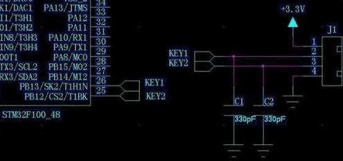
7) Isolation should be paid attention to between high current signals, high voltage signals and small signals (the isolation distance is related to the withstand voltage. Usually, the distance on the board is 2 mm at 2 kV, and it should be increased in proportion. For example, if it is to withstand a 3 kV withstand voltage test, the distance between the high and low voltage lines should be more than 3.5 mm. In many cases, in order to avoid creepage, slots are also opened between the high and low voltage on the printed circuit board).
3 Circuit design in PCB
When designing electronic circuits, the actual performance of the product is considered more, and the electromagnetic compatibility characteristics, electromagnetic interference suppression and electromagnetic anti-interference characteristics of the product are not considered too much. When using the circuit schematic to layout the PCB, in order to achieve the purpose of electromagnetic compatibility, necessary measures must be taken, that is, necessary additional circuits must be added on the basis of the circuit schematic to improve the electromagnetic compatibility performance of the product. The following circuit measures can be used in actual PCB design:
1) A resistor can be connected in series on the PCB trace to reduce the jump rate of the upper and lower edges of the control signal line.
2) Try to provide some form of damping (high-frequency capacitors, reverse diodes, etc.) for relays, etc.
3) The signal entering the printed circuit board should be filtered, and the signal from the high noise area to the low noise area should also be filtered. At the same time, the terminal resistor should be used in series to reduce signal reflection.
4) The unused end of the MCU should be connected to the power supply or ground through the corresponding matching resistor, or defined as the output end. The terminals that should be connected to the power supply and ground on the integrated circuit should be connected, and should not be left floating.
5) The input terminals of the unused gate circuit should not be left floating, but connected to the power supply or ground through the corresponding matching resistor. The positive input terminal of the unused op amp should be grounded, and the negative input terminal should be connected to the output terminal.
6) Set a high-frequency decoupling capacitor for each integrated circuit. A small high-frequency bypass capacitor should be added to the side of each electrolytic capacitor.
7) Use large-capacity tantalum capacitors or polyester capacitors instead of electrolytic capacitors as charging and discharging energy storage capacitors on the circuit board. When using tubular capacitors, the outer shell should be grounded.
4 Conclusion
With the development of science and technology, the miniaturization and intelligence of various electronic equipment have become the mainstream trend. At the same time, the operating environment of electronic products or equipment will become more and more complex, and anti-interference technology and electromagnetic compatibility technology also require continuous development and maturity.