Electromagnetic radiation detection technology in high-speed PCB design
Currently, most hardware engineers still design PCBs based on experience. During the debugging process, many signal lines or chip pins that need to be observed are buried in the middle layer of the PCB, and cannot be detected using tools such as oscilloscopes. If the product fails the functional test, they have no effective means to find the cause of the problem.
To verify the EMC characteristics of the product, the product can only be measured in a standard electromagnetic compatibility measurement room. Since this measurement can only measure the external radiation of the product, even if it fails, it cannot provide useful information for solving the problem. Therefore, engineers can only modify the PCB based on experience and repeat the test. This test method is very expensive and may delay the time to market of the product.
Of course, there are many high-speed PCB analysis and simulation design tools that can help engineers solve some problems, but there are still many limitations in the device model.
For example, the IBIS model that can solve the signal integrity (SI) simulation has many devices without models or inaccurate models. To accurately simulate EMC problems, SPICE models must be used, but almost all ASICs currently cannot provide SPICE models. Without SPICE models, EMC simulation cannot take into account the radiation of the device itself (the radiation of the device is much greater than that of the transmission line). In addition, simulation tools often have to compromise between accuracy and simulation time. Tools with relatively high accuracy require a long calculation time, while tools with fast simulation speed have low accuracy. Therefore, using these tools for simulation cannot completely solve the mutual interference problem in high-speed PCB design.
We know that the return path of high-frequency signals in multi-layer PCBs should be on the reference ground plane (power layer or ground layer) adjacent to the signal line layer.
Such return and impedance are minimal, but there will be segmentation and hollowing in the actual ground layer or power layer, which will change the return path, resulting in a larger return area, causing electromagnetic radiation and ground bounce noise. If engineers can clearly understand the current path, they can avoid large return paths and effectively control electromagnetic radiation. However, the signal return path is determined by many factors such as signal line routing, PCB power and ground distribution structure, power supply point, decoupling capacitors and device placement and quantity. Therefore, it is very difficult to theoretically determine the return path of a complex system.
Therefore, it is very critical to eliminate the problem of radiation noise during the design stage. We can see the waveform of the signal with an oscilloscope, which can help solve the signal integrity problem. So is there any equipment that can see the “graph” of radiation and the return current on the circuit board?
Electromagnetic field high-speed scanning measurement technology
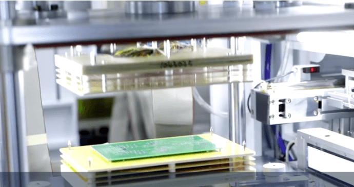
Among various electromagnetic radiation measurement methods, there is a near-field scanning measurement method that can solve this problem. This method is designed based on the principle that electromagnetic radiation is formed by the high-frequency current loop on the device under test (DUT). For example, the electromagnetic radiation scanning system Emscan of Canada EMSCAN Company is made according to this principle. It uses H-field array probes (32×40=1280 probes) to detect the current on the DUT. During the measurement, the DUT is placed directly on the scanner. These probes can detect changes in the electromagnetic field caused by changes in high-frequency current. The system can provide a visual image of the spatial distribution of RF current on the PCB.
Emscan electromagnetic compatibility scanning system has been widely used in industrial fields such as communications, automobiles, office appliances and consumer electronics. Through the current density map provided by the system, engineers can find areas with EMI problems and take corresponding measures before conducting electromagnetic compatibility standard tests.
Near-field scanning principle Emscan’s measurement is mainly carried out in the active near-field area (r<<λ/2π).
Most of the radiation signals emitted by the DUT are coupled to the magnetic field probe, and a small amount of energy diffuses into the free space. The magnetic field probe couples the magnetic flux lines of the near H field and the current on the PCB. In addition, it also obtains some trace components of the near E field.
Large current and low voltage current sources are mainly related to magnetic fields, while high voltage and low current voltage sources are mainly related to electric fields.
On PCBs, pure electric fields or pure magnetic fields are rare. In RF and microwave circuits, the input impedance of the circuit and the impedance of the microstrip or microstrip line used for connection are designed to be 50 ohms. This low impedance design allows these components to generate large current and low voltage changes. In addition, the trend of digital circuits is also to use logic devices with lower voltage differences. At the same time, the magnetic field wave impedance in the active near-field area is much smaller than the electric field wave impedance. Combining these factors, most of the energy in the active near-field area of PCBs is contained in the near magnetic field. Therefore, the magnetic field ring used by the Emscan scanning system is suitable for near-field diagnosis of these PCBs.
All loops are the same, but they are
located in different positions in the feedback network, so the feedback network can sense the response of each loop, and the response of each loop relative to the reference source is measured and considered as a filter transfer function. In order to ensure the linearity of the measurement, Emscan measures the inverse of this transfer function.
Due to the use of array antennas and electronic automatic switching antenna technology, the measurement speed is greatly accelerated, thousands of times faster than the manual single probe measurement solution, and hundreds of times faster than the automatic single probe measurement solution, which can quickly and effectively determine the effect before and after the circuit modification. Fast scanning technology and its advanced amplitude retention scanning technology and synchronous scanning technology enable the system to effectively capture transient events. At the same time, it uses technology that can improve the measurement accuracy of the spectrum analyzer, which improves the accuracy and repeatability of the measurement.
*Measurement method for estimating PCB near-field radiation interference
The inspection of PCB radiation interference can be carried out in several steps. First, determine the area to be scanned, then select a probe that can fully sample the scanning area (grid 7.5mm), perform spectrum scanning in the frequency range of 100kHz to 3GHz, and store the maximum level of each frequency point. Note that the larger frequency points can be further checked in the scan area using spatial scanning, which can locate interference sources and critical circuit paths.
The board under test must be as close to the scanner board as possible, because the received signal-to-noise ratio decreases with increasing distance, and there is also a “separation” effect. In actual measurements, this distance should be less than 1.5cm. We can see that the measurement of the component surface may sometimes cause problems due to the height of the component, so the height of the component must be considered to correct the measured voltage level. In basic inspections, the separation distance correction factor needs to be considered.
We can get the measurement results quickly, but these results cannot * judge whether the product meets the EMC characteristics, because the value it measures is the electromagnetic near field generated by the high-frequency current on the PCB board. Standard EMC testing is required to be carried out in an open field (OATS) or in a dark room, with a distance of 3 meters (i.e. far field).
Although Emscan measurements cannot replace standard EMC tests, practice has shown that it does have many uses. By analyzing the measurement results, many conclusions can be drawn to facilitate the subsequent development of products. In addition to the voltage level, the following information is also very important: the interference generation point, the interference distribution, the interference conduction path covering a large area, the interference is limited to a narrow area on the PCB, and the coupling between the internal structure or adjacent I/O modules, etc., and the effect of separating digital circuits and analog circuits can also be seen.
The above measurements can be used as a standard for evaluating the quality of PCB design. Furthermore, if we already know the EMC characteristics of a similar PCB, we can make a more reliable evaluation of the EMC characteristics in the early stage of product development, such as whether shielding measures should be adopted.
It is particularly worth mentioning that the electromagnetic field high-speed scanning system can also reveal transient EMI problems, which are often not detected in electromagnetic compatibility measurements, but they will affect the performance and reliability of the product.
Evaluation of PCB anti-interference performance
In actual use, all electronic devices will be interfered by electromagnetic fields. If a device does not meet the anti-interference requirements and is not shielded, the performance of the device will be affected by electromagnetic interference. Facts show that the frequency of interference signals may be hundreds of MHz, and these interferences are mainly coupled through connected conductors, so the anti-interference design of I/O modules is very important. In order to enhance the anti-interference performance of the product, sometimes it is necessary to add filtering and other means, which means that the cost of the product will increase. From this perspective, it is very important to find a solution that can optimize all circuits and components.
By appropriately modifying the measurement method mentioned above, the anti-interference performance of the product can be correctly estimated during the product development and testing stage.
The improved method is as follows: Place the PCB on the scanner board for spectrum scanning to determine the interference frequency of the PCB, and then couple the sinusoidal interference signal of this frequency to the I/O line or conductor with a clip or appropriate coupling device (such as T-LISN used on balanced lines), use a generator with a step size of 10MHz, a frequency range of 10MHz to 150MHz (avoid overlapping with the interference frequency of the PCB board), and a power of -20 to 0dBm (depending on the type of coupling device and PCB), and perform a spatial scan at a frequency consistent with the added interference signal. The distribution of interference signals from the coupling point to the PCB can be clearly seen in the spatial scanning diagram. The spatial scanning results can then be interpreted based on the following principles, including which areas on the PCB have coupled interference signals, the effectiveness of inserted filters (attenuating interference signals), coupling conditions of adjacent I/O conductors, and the effectiveness of the PCB ground layer or area.

